Packaging structure of a driving circuit for a liquid crystal display device and packaging method of a driving circuit for a liquid crystal display device

a technology of driving circuit and liquid crystal display device, which is applied in the direction of conductive pattern formation, semiconductor/solid-state device details, instruments, etc., can solve the problems of increasing the manufacturing process of driving circuit and module, and achieve the effect of not increasing the volume of the liquid crystal display devi

Inactive Publication Date: 2005-04-21
LG DISPLAY CO LTD
View PDF21 Cites 20 Cited by
  • Summary
  • Abstract
  • Description
  • Claims
  • Application Information

AI Technical Summary

Benefits of technology

[0017] An advantage of the present invention is to provide a packaging structure of a driving circuit that is suitable for a high-resolution liquid crystal display device.
[0018] Another advantage of the present invention is to provide a packaging method of a driving circuit for the high-resolution liquid crystal display device.
[0019] Additional features and advantages of the invention will be set forth in the description which follows, and in part will be apparent from the description, or may be learned by practice of the invention. These and other advantages of the invention will be realized and attained by the structure in the written description and claims hereof as well as the appended drawings.
[0020] To achieve these and other advantages and in accordance with the purpose of the present invention, as embodied and broadly described, a packaging structure of a driving circuit for a liquid crystal display device comprises a base film, a plurality of first metal lines being formed on the base film and being disposed with a certain distance between neighboring first metal lines, an insulating film on the first metal lines, the insulating film exposing both ends of the first metal lines, and a plurality of second metal lines on the insulating film, the second metal lines being formed parallel to the first metal lines. The first metal line consists of two terminals at both ends of the first metal line, a connection part between the two terminals; the connection part being narrower in width than the terminals. The second metal lines correspond to the connection parts of the first metal lines and are disposed in an alternating order with the connection parts of the first metal lines. The second metal line consists of two terminals at both ends of the second metal line and a connection part between the two terminals; the width of the connection part of the second metal line being wider than a width of the connection part of the first metal line. The packaging structure of the driving circuit of the liquid crystal display device may further include an overcoat layer that exposes both ends of the first metal lines and the second metal lines, and a drive integrated circuit that is connected to the terminals at one end of the first metal lines and the adjacent terminals of the second metal lines. The first metal line and the second metal line may be formed of copper (Cu).
[0021] A packaging method of a driving circuit of a liquid crystal display device comprises the steps of preparing a base film, forming a plurality of first metal lines on the base film, forming an insulating film on the first metal lines, and exposing both ends of the first metal lines, forming a plurality of second metal lines on the insulating film, and forming an overcoat layer on the second metal lines, the overcoat layer exposing both ends of the first metal lines and the second metal lines.
[0022] According to the present invention, two output metal lines are formed in a pitch by forming a double layered output metal line of the chip on film (COF) (or the tape carrier package (TCP)) achieving a high-resolution liquid crystal display device that has more than 300 pixels per inch. Accordingly, the present invention can provide a compact high-resolution liquid crystal display device without increasing a volume of the liquid crystal display device.

Problems solved by technology

However, as the volume of the liquid crystal panel increases, the cost increases for the manufacturing process of a driving circuit and module.

Method used


Image

  • Packaging structure of a driving circuit for a liquid crystal display device and packaging method of a driving circuit for a liquid crystal display device
  • Packaging structure of a driving circuit for a liquid crystal display device and packaging method of a driving circuit for a liquid crystal display device
  • Packaging structure of a driving circuit for a liquid crystal display device and packaging method of a driving circuit for a liquid crystal display device

Examples


Embodiment Construction

[0035] Reference will now be made in detail to the illustrated embodiment of the present invention, which is illustrated in the accompanying drawings.

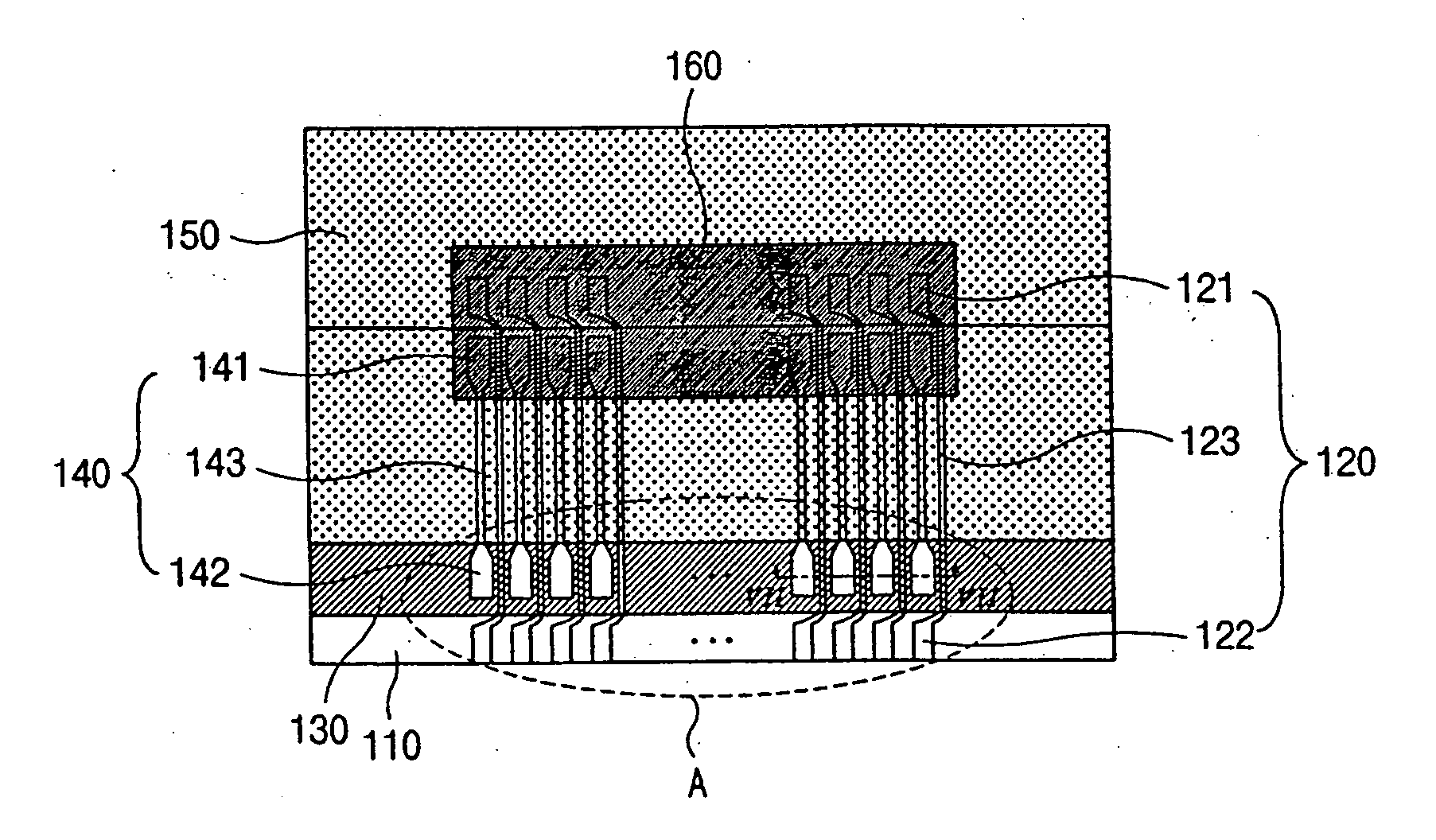
[0036]FIG. 6 is a plan view illustrating a packaging structure of a chip on film (COF) of a data driving circuit according to the present invention. FIG. 7 is a cross-sectional view taken along VII-VII of FIG. 6. Because the structure of input metal lines has been described before, the following description of output metal lines will be described with reference to related figures.

[0037] In FIG. 6 and FIG. 7, a plurality of first output lines 120 is formed on a base film 110 with a specific distance between the first output lines 120. The first output line 120 consists of two terminals 121 and 122 at respective ends of the first output line 120 and a connection part 123 that connects the two terminals and has a narrower width than the terminals 121 and 122. The connection part 123 is positioned to a right side of the terminals 121 and...


PUM

PropertyMeasurementUnit
insulatingaaaaaaaaaa
widthaaaaaaaaaa
weightaaaaaaaaaa

Abstract

A packaging structure of a driving circuit for a liquid crystal display device comprises a base film, a plurality of first metal lines being formed on the base film and being disposed with a certain distance between neighboring first metal lines, an insulating film on the first metal lines, the insulating film exposing both ends of the first metal lines, and a plurality of second metal lines on the insulating film, the second metal lines being formed parallel to the first metal lines.

Description

[0001] This application claims the benefit of Korean Patent Application No. 2001-15563, filed on Mar. 26, 2001 in Korea, which is hereby incorporated by reference for all purposes as if fully set forth herein. BACKGROUND OF THE INVENTION [0002] 1. Field of the Invention [0003] The present invention relates to a liquid crystal display (LCD) device and more particularly, to a packaging structure of a driving circuit for a liquid crystal display device and a packaging method of the driving circuit for the liquid crystal display device. [0004] 2. Discussion of the Related Art [0005] Flat panel display devices, that are thin, low weight and low power consumption, have been required as the information age rapidly evolves. The liquid crystal display device is widely used for notebook computers and desktop monitors, etc. because of its superior resolution, color image display and quality of displayed images. [0006] Generally, the liquid crystal display device has upper and lower substrates,...

Claims


Application Information

Patent Timeline
Patent Type & Authority Applications(United States)
IPC IPC(8): G02F1/13G02F1/1345H01L23/498H05K1/11H05K3/36H05K3/46
CPCG02F1/13452Y10T29/49117H05K1/117H05K1/118H05K3/361H05K3/4644H05K2201/0919H05K2201/09409H05K2201/09727H01L2924/0002H01L23/4985Y10T29/49155Y10T29/49126H01L2924/00G02F1/1345
Inventor HWANG, KWANG-JOKIM, WOO-HYUN
Owner LG DISPLAY CO LTD
Why Eureka
Try Eureka