Formation of self-aligned contact plugs

a technology of contact plugs and plugs, which is applied in the direction of semiconductor/solid-state device manufacturing, basic electric elements, electric apparatus, etc., can solve the problems of etch selectivity, contact width and sidewall spacer thickness, and the difficulty of balancing the thickness of the polymer layer, and the difficulty of removing doped oxide relative to un-doped oxid

Inactive Publication Date: 2005-04-21
MICRON TECH INC
View PDF9 Cites 68 Cited by
  • Summary
  • Abstract
  • Description
  • Claims
  • Application Information

AI Technical Summary

Problems solved by technology

Removing doped oxide relative to un-doped oxide can be more difficult than removing an oxide relative to nitrite.
As such, if too high of a selectivity is used the contact opening can become blocked with the polymer layer.
Balancing the thickness of the polymer layer, etch selectivity, contact width and the thickness of the sidewall spacer is challenging.
Prior etch processes have been limited to a selectivity of oxide to nitride in the range of less than 40:1.

Method used


Image

  • Formation of self-aligned contact plugs
  • Formation of self-aligned contact plugs
  • Formation of self-aligned contact plugs

Examples


Embodiment Construction

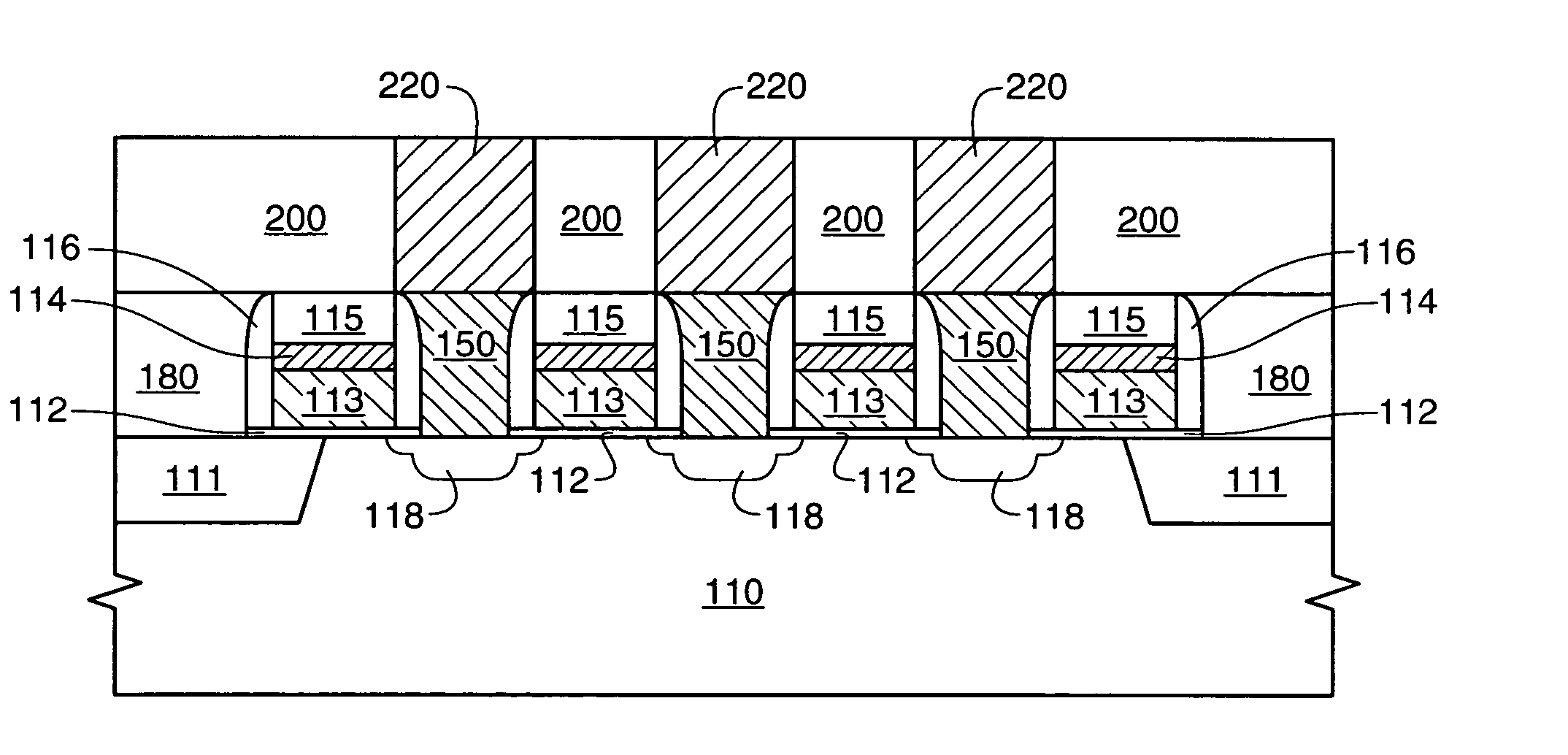
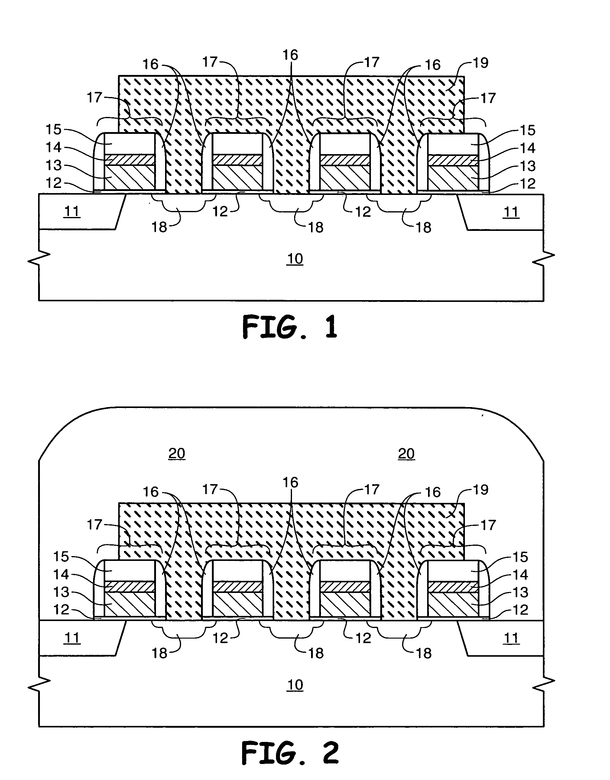
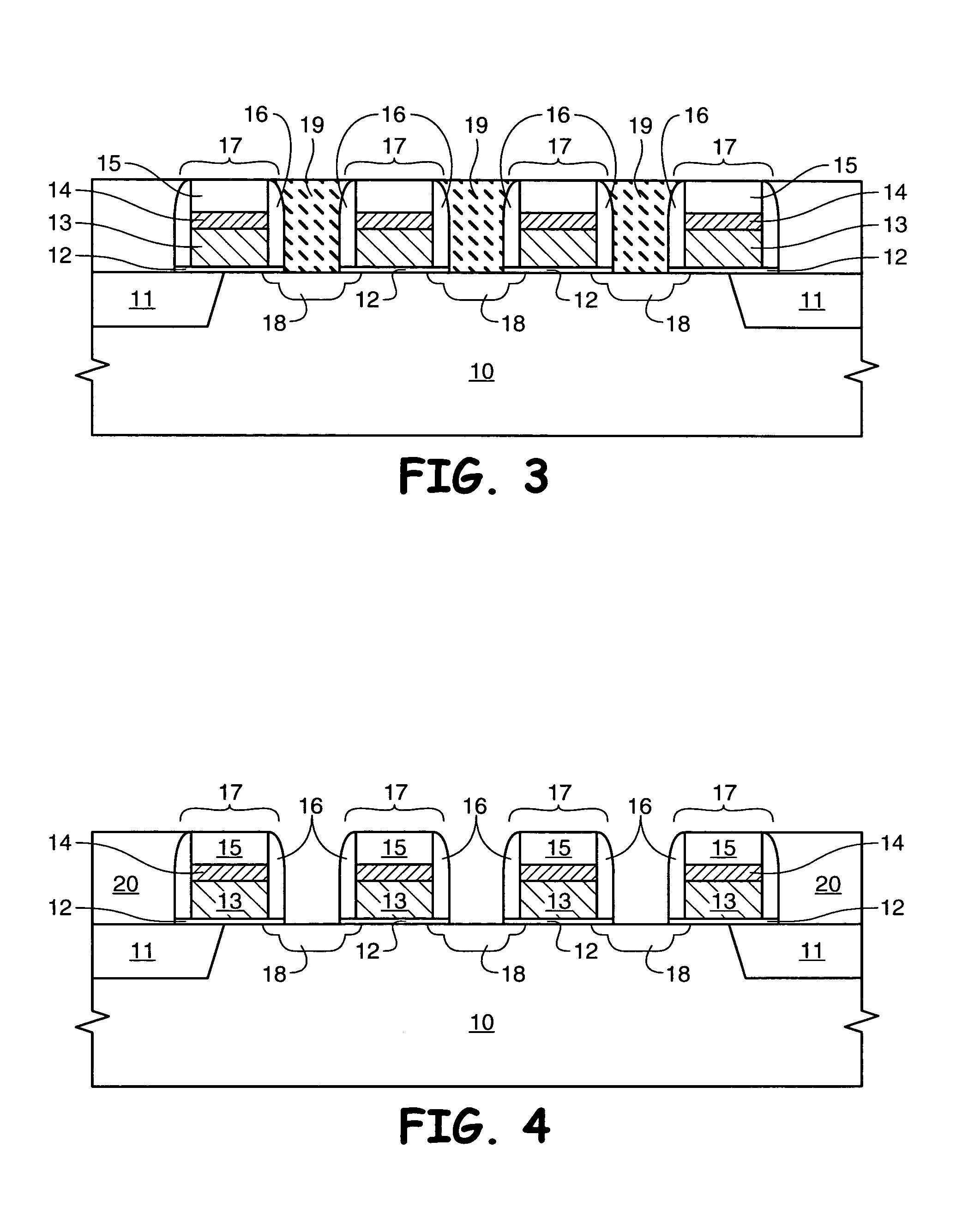
[0034] Embodiments of the present invention provide methods of forming transistor contacts without degrading sidewall spacers. In some embodiments either a photoresist or amorphous carbon material is used to fill a region between transistor gate stacks. The photoresist or amorphous carbon material can be removed to expose the source / drain contact area without substantial sacrificial removal of the sidewall spacer. That is, the photoresist or amorphous carbon material can be removed with greater selectivity to the spacer material than prior materials. For example, a dry develop process can be performed to remove the amorphous carbon material. It will be appreciated by those in the art with the benefit of the present disclosure that the present invention is not limited to photoresist or amorphous carbon material but can be implemented with other materials that can be removed without etching a sidewall spacer. For example, a filler material can be used that can be removed with a select...


PUM


Abstract

Methods of forming a contact structure for semiconductor assemblies are described. One method provides process steps to create an inner dielectric isolation layer after the contact region is protected, which is followed by the formation of the self-aligned contact structures. A second method provides process steps to create an inner dielectric isolation layer after the self-aligned contact structures are formed.

Description

FIELD OF THE INVENTION [0001] This invention relates to semiconductor fabrication processing and, more particularly, to methods for forming self-aligned contact plugs for semiconductor devices, such as dynamic random access memories (DRAMs). BACKGROUND OF THE INVENTION [0002] The continuing trend of scaling down integrated circuits has motivated the semiconductor industry to consider new techniques for fabricating precise components at sub-micron levels. One important area in semiconductor fabrication is forming the interconnecting structure within the integrated circuit and particularly connection between a transistor and other devices. [0003] As is the case for most semiconductor integrated circuitry, circuit density is continuing to increase at a fairly constant rate. In semiconductor devices it may be advantageous to build contact plugs for interlayer connections having high aspect ratio structures, as circuit density will be enhanced. In that light, the ability to precisely ali...

Claims


Application Information

Patent Timeline
Patent Type & Authority Applications(United States)
IPC IPC(8): H01L21/44H01L21/60
CPCH01L21/76897
Inventor KIM, HYUN T.BURGESS, BYRON N.
Owner MICRON TECH INC
Why Eureka
Try Eureka