Image display device

a technology of image display and display device, which is applied in the direction of static indicating device, identification means, instruments, etc., can solve the problems of significant voltage drop and degrade image quality, and achieve the effect of reducing variations in brightness of light emitting elements and good image quality

Active Publication Date: 2005-04-28
SAMSUNG DISPLAY CO LTD +1
View PDF7 Cites 204 Cited by
  • Summary
  • Abstract
  • Description
  • Claims
  • Application Information

AI Technical Summary

Benefits of technology

[0023] According to the present invention, the image display device that reduces variations in brightness of the light emitting element

Problems solved by technology

For an image display device having a large screen, the power source line is long and, consequently, such voltage drop becomes significant.
In an image display device using the pixel circ

Method used


Image

  • Image display device
  • Image display device
  • Image display device

Examples


embodiment 1

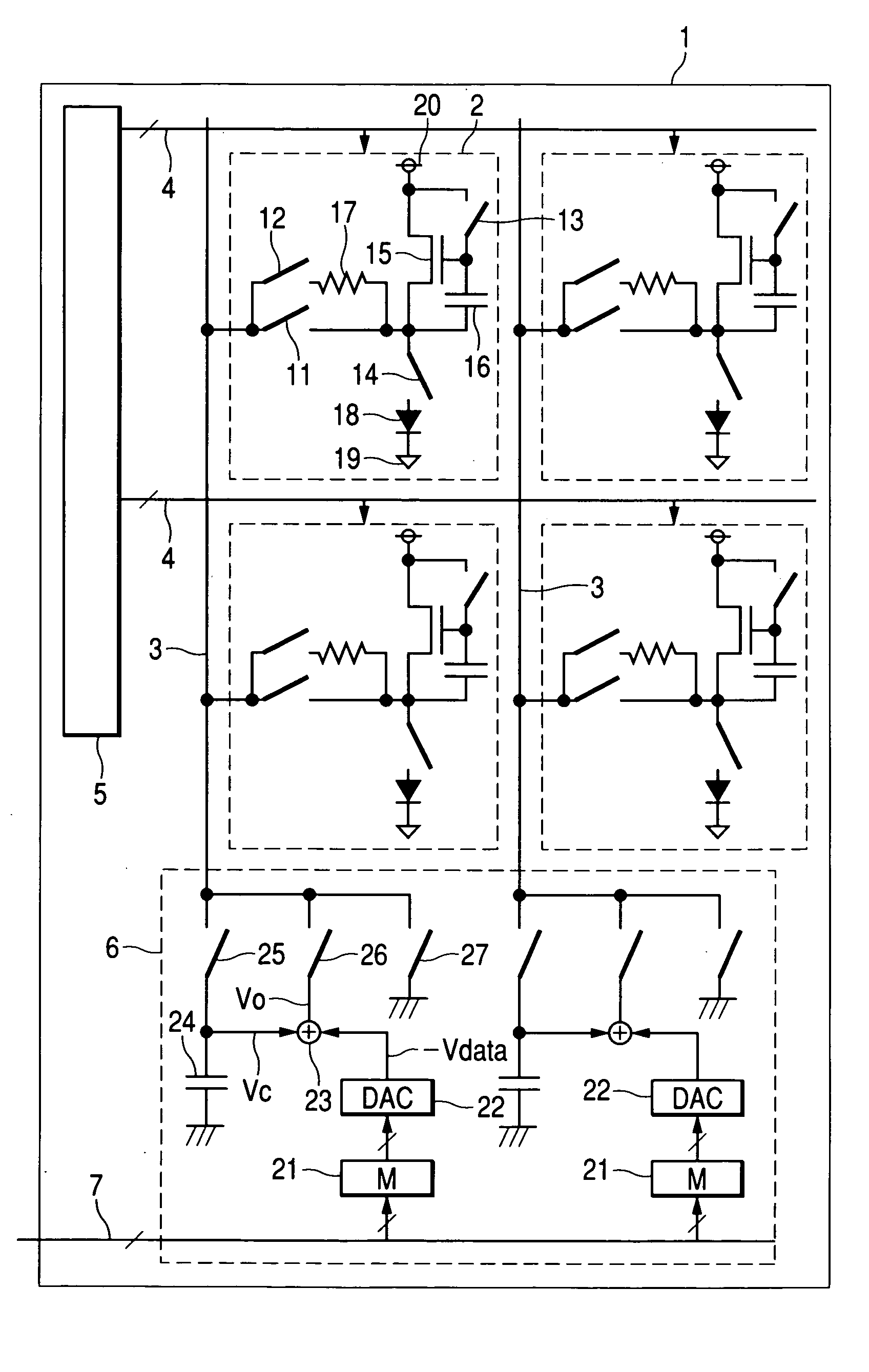
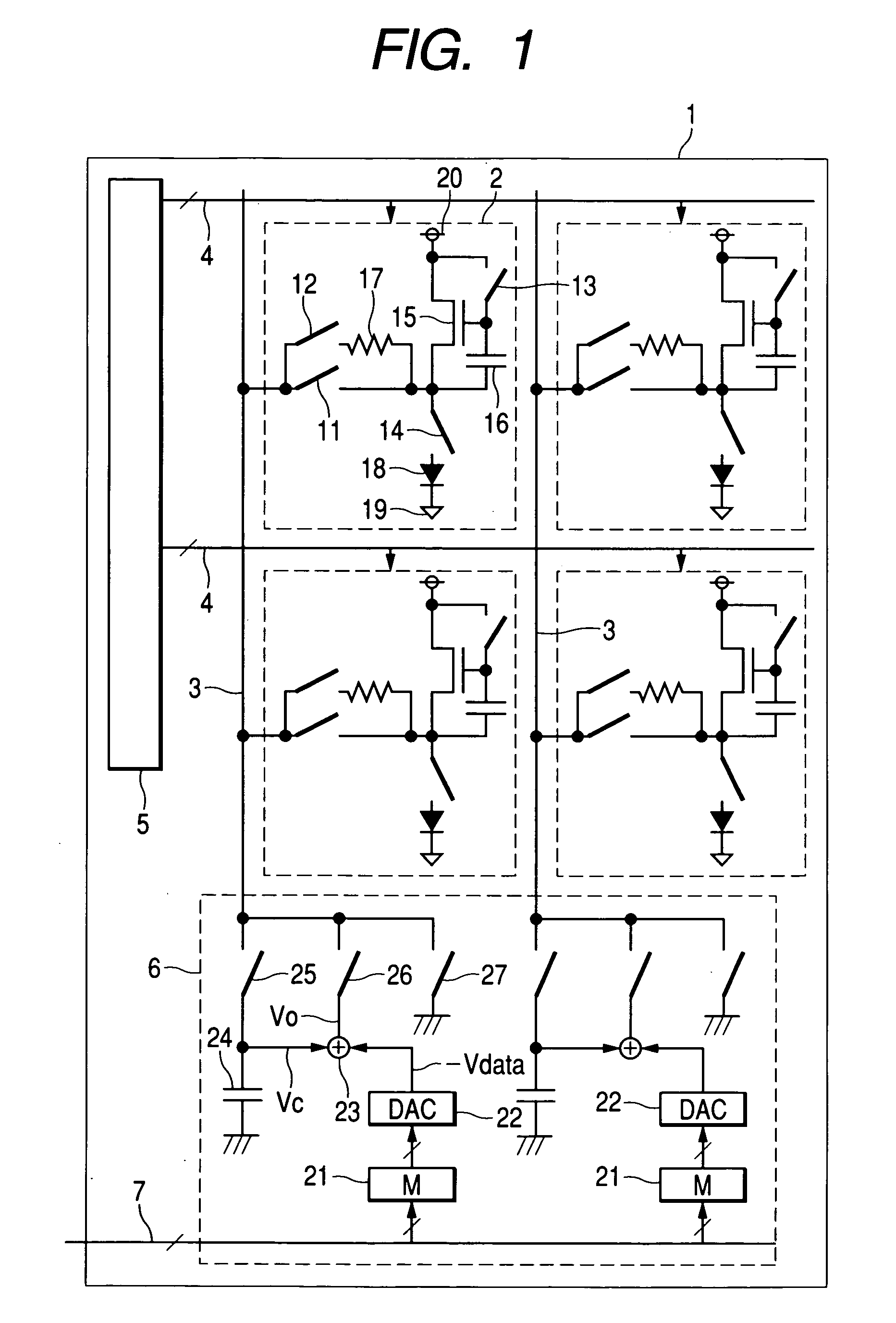
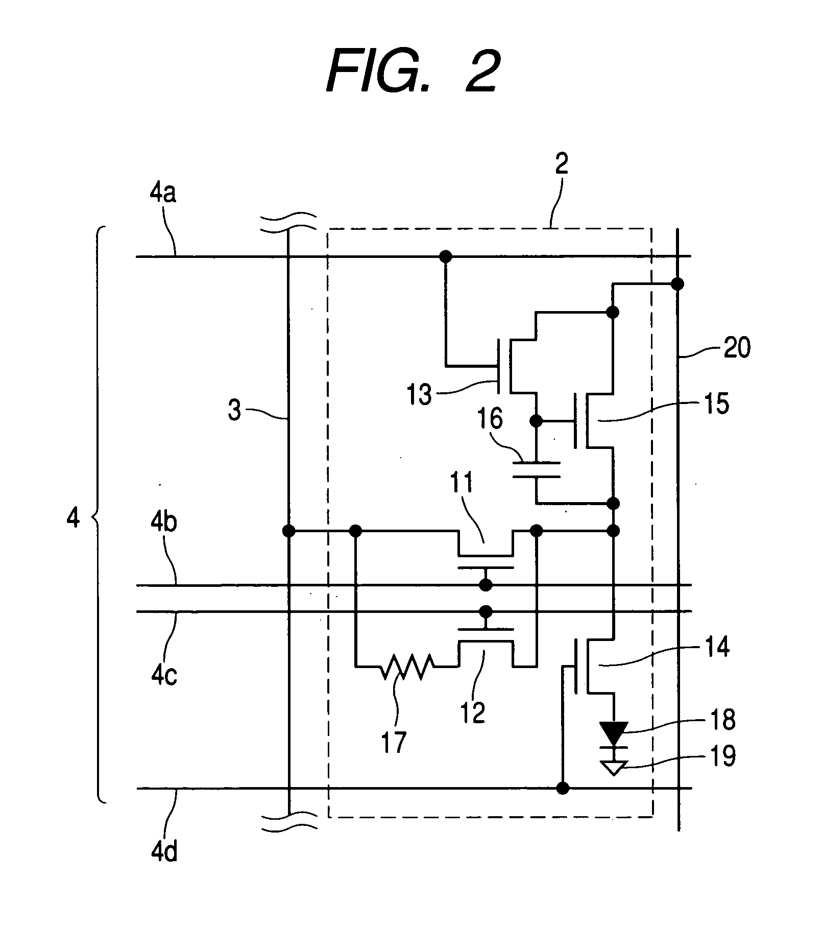
[0038]FIG. 1 is a circuitry diagram showing a preferred Embodiment 1 of the image display device according to the present invention. On a glass substrate 1, a plurality of pixel circuits 2, a plurality of signal lines 3, a plurality of scan buses 4, and a scanning circuit 5 are formed.

[0039] The pixel circuits 2 are arranged in a matrix of two columns by two rows. The reason why the number of the pixel circuits 2 is 2×2=4 is merely for simplifying explanation. For, for example, a screen resolution of a color Video Graphics Array (VGA), the number of pixels could be 1920 columns (640 columns×3 colors) by 480 rows. Each signal line 3 connects to individual pixel circuits 2 arranged in one column and each scan bus 4 connects to individual pixel circuits 2 arranged in one row. The scanning circuit 5 connects to all the scan buses 4 and outputs signals to the scan buses 4. In addition, a driver IC 6 is bonded on the surface of the glass substrate 1 and has connections to the signal line...

embodiment 2

[0066]FIG. 5 is a circuitry diagram showing a preferred Embodiment 2 of the image display device according to the present invention. On a glass substrate 41, a plurality of pixel circuits 42, a plurality of dummy pixel circuits 49, a plurality of signal lines 43, a plurality of resistive wiring lines 48, a plurality of scan buses 44, and a scanning circuit 45 are formed. The pixel circuits 42 are arranged in a matrix of two columns by three rows. The reason why the number of the pixel circuits 42 is 2×3=6 is merely for simplifying explanation. For, for example, a screen resolution of the color VGA, the number of pixels could be 1920 columns (640 columns×3 colors) by 480 rows. Each signal line 43 and each resistive wiring line 48 are connected to individual pixel circuits 42 and dummy pixel circuits 49 arranged in one column and each scan bus 44 is connected to individual pixel circuits 42 and dummy pixel circuits 49 arranged in one row. The scanning circuit 45 has connections to all...

embodiment 3

[0090] In the following, a preferred Embodiment 3 of the invention will be described, involving an example of modification to Embodiments 1 and 2 and an adder circuit configuration example.

[0091] While all the TFTs in an pixel circuit are n-channel TFTs in Embodiments 1 and 2 described hereinbefore, it is obvious that the above TFTs can be configured as p-channel TFTs by reversing the voltage polarity at all nodes, the direction of current, and the anode and cathode of an EL element.

[0092]FIG. 10 shows the configuration of the adder circuit 23 used in the above Embodiments 1 and 2. The adder circuit 23 is comprised of an op-amp circuit 81 and resistors 82 and 83 having a resistance value of r. The adder circuit 23 generates a voltage that is obtained by Equation 6 below as the output voltage Vo.

Vo=Vc−(r / r)Vdata=Vc−Vdata  (Equation 6)

[0093] Thus, the adder circuit shown in FIG. 10 is able to add the voltage −Vdata and the voltage Vc on the capacitor 24.

[0094]FIG. 11 shows a circ...


PUM


Abstract

The present invention provides an image display device that reduces variations in brightness of the light emitting elements included in the device due to a voltage drop on the power source line of the device and TFT threshold voltage variations and displays good quality images. The image display device is equipped with a pixel circuit voltage detecting means to selectively output a voltage internal to a pixel circuit included in each of a plurality of pixels of the device to a signal line to which the pixel circuit connects. Its drive circuit is equipped with a voltage addition means to add the signal line voltage and a signal voltage corresponding to image data to be displayed and output a sum voltage to the signal line again.

Description

BACKGROUND OF THE INVENTION [0001] 1. Field of the Invention [0002] The present invention relates to image display devices and, more particularly, to an image display device in which a light emitting element is used in a pixel. [0003] 2. Description of the Prior Art [0004] As an image display device employing light emitting elements for pixels, an EL display using electro-luminescence (hereinafter abbreviated to EL) elements has been reported. Besides, in an active matrix type EL display, wiring lines for signal and current transmission are formed in the shape of a matrix and pixel circuits are respectively built into pixels, wherein each pixel circuit is formed of thin-film transistors (hereinafter abbreviated to TFTs) which are active elements besides a light emitting element. [0005] There are two methods of controlling the light emitting brightness of an EL element: a method in which voltage supplied to the EL element through the pixel circuit is controlled and a method in which ...

Claims


Application Information

Patent Timeline
IPC IPC(8): H01L51/50G09F9/30G09G3/10G09G3/20G09G3/30G09G3/32G09G5/10H05B33/14
CPCG09G3/3233G09G3/325G09G3/3291G09G2300/0842G09G2300/0861G09G2320/043G09G2310/0251G09G2310/027G09G2320/0223G09G2320/0233G09G2320/0295G09G2310/0248G08G1/095G08G1/096
Inventor KAGEYAMA, HIROSHIAKIMOTO, HAJIME
Owner SAMSUNG DISPLAY CO LTD
Why Eureka
Try Eureka