Image display device

a technology of image display and display device, which is applied in the direction of static indicating device, identification means, instruments, etc., can solve the problems of significant voltage drop and degrade image quality, and achieve the effect of reducing variations in brightness of light emitting elements and good image quality

Active Publication Date: 2006-03-14
SAMSUNG DISPLAY CO LTD +1
View PDF8 Cites 16 Cited by
  • Summary
  • Abstract
  • Description
  • Claims
  • Application Information

AI Technical Summary

Benefits of technology

[0023]According to the present invention, the image display device that reduces variations in brightness of the light emitting elements due to a voltage drop on the power source line and TFT threshold voltage variations and displays good quality images can be realized.

Problems solved by technology

For an image display device having a large screen, the power source line is long and, consequently, such voltage drop becomes significant.
In an image display device using the pixel circuits exemplified in FIG. 13, when the EL element brightness per pixel is influenced as above, unevenness in lightness is observed on an image displayed, which degrades the image quality.

Method used


Image

  • Image display device
  • Image display device
  • Image display device

Examples


embodiment 1

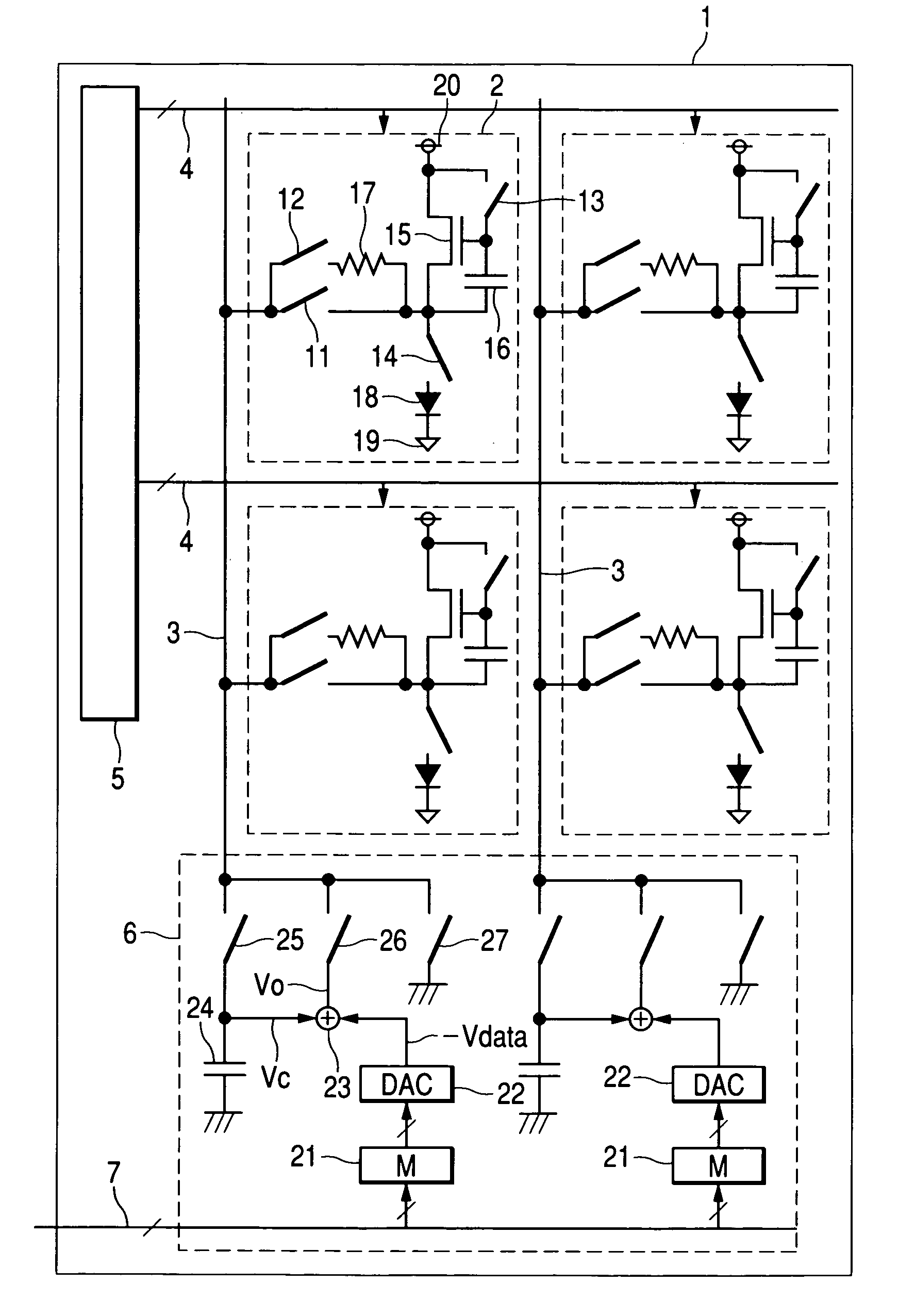
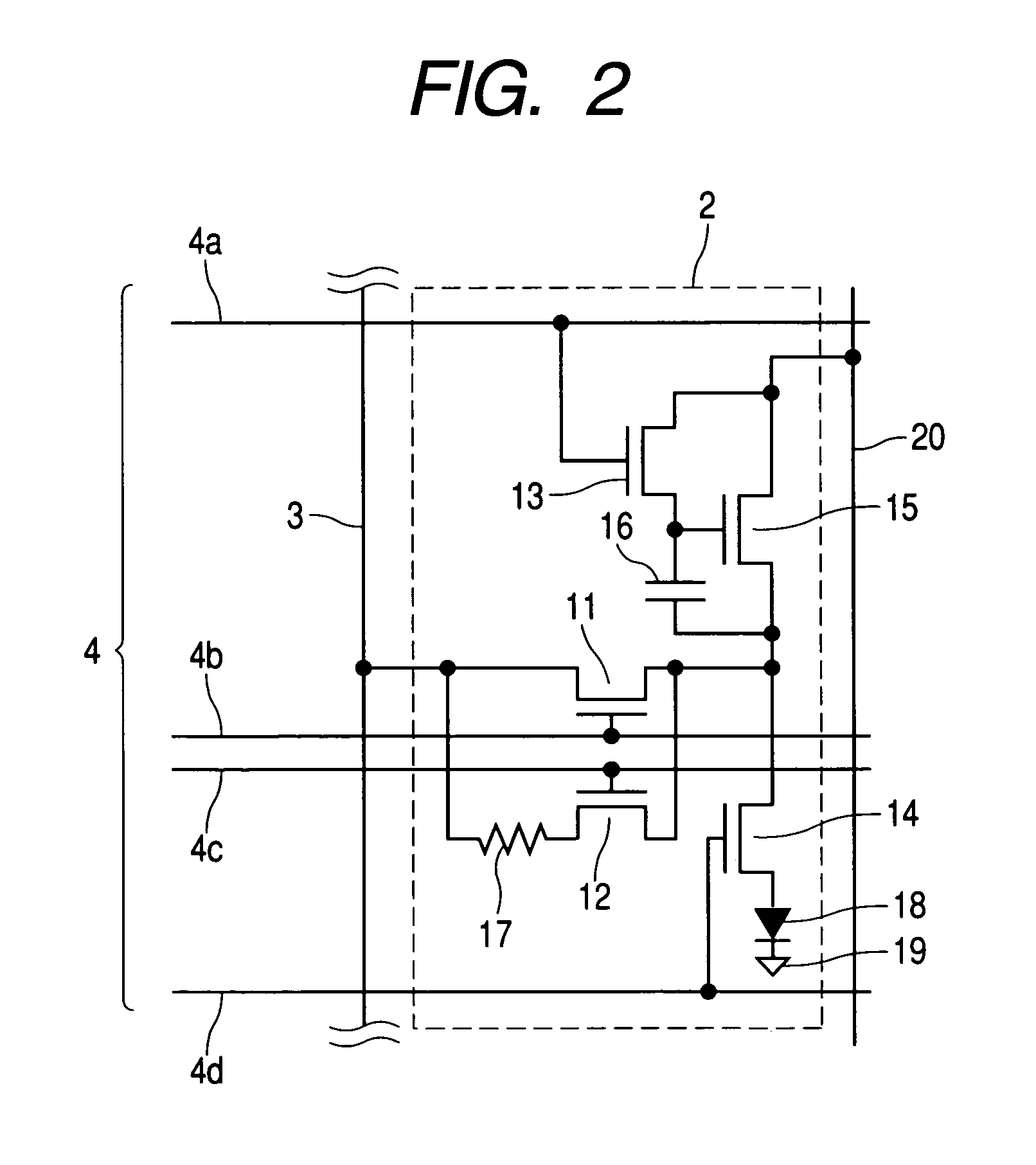
[0047]FIG. 4 shows the waveforms of drive signals on a scan buses 4, ON / OFF operations of the switches on the driver IC 6, and voltages and currents generated in the internal circuitry of the display device to drive the image display device of The following explanation for FIG. 4 will be made, assuming an instance of driving a top left pixel circuit typical of the plurality of pixel circuits 2 shown in FIG. 1.

[0048]L(4a), L(4b), L(4c), and L(4d) represent the waveforms of drive signals which the scanning circuit generates and outputs to the scan lines 4a to 4b, respectively. The signals of L(4a) to L(4d) are two-value logic voltage signals. During a high voltage signal state (hereinafter abbreviated to H), the associated TFT switch is ON. During a low voltage signal state (hereinafter abbreviated to L), the associated TFT switch is OFF. S(25) S(26), and S(27) represent transition of the ON / OFF states of the switches 25 to 27 included in the driver IC 6, respectively.

[0049]Vsig repr...

embodiment 2

[0075]FIG. 8 shows the ON / OFF operations of the TFT switches 51 to 54, ON / OFF operations of the switches on the driver IC 6, and voltages and currents generated in the internal circuitry of the display device to drive the image display device of The following explanation for FIG. 8 will be made, assuming an instance of driving a top left pixel circuit typical of the plurality of pixel circuits 42 shown in FIG. 5. Marked periods in 9-ABC represent different states of the TFT switches 51 to 54; periods “a,”“b,” and “c” correspond to the states shown in FIGS. 9A, 9B, and 9C, respectively. FIGS. 9A to 9C are the drawings of the top left pixel circuit and its adjacency extracted from FIG. 5 in the different periods. Period “x” denotes a state that all the TFT switches are OFF (not shown in FIGS. 9A to 9C). S(25), S(26), and S(27) in FIG. 8 represent transition of the ON / OFF states of the switches 25 to 27 included in the driver IC 6, respectively. Vsig represents a voltage on the releva...


PUM


Abstract

The present invention provides an image display device that reduces variations in brightness of the light emitting elements included in the device due to a voltage drop on the power source line of the device and TFT threshold voltage variations and displays good quality images. The image display device is equipped with a pixel circuit voltage detecting means to selectively output a voltage internal to a pixel circuit included in each of a plurality of pixels of the device to a signal line to which the pixel circuit connects. Its drive circuit is equipped with a voltage addition means to add the signal line voltage and a signal voltage corresponding to image data to be displayed and output a sum voltage to the signal line again.

Description

BACKGROUND OF THE INVENTION[0001]1. Field of the Invention[0002]The present invention relates to image display devices and, more particularly, to an image display device in which a light emitting element is used in a pixel.[0003]2. Description of the Prior Art[0004]As an image display device employing light emitting elements for pixels, an EL display using electro-luminescence (hereinafter abbreviated to EL) elements has been reported. Besides, in an active matrix type EL display, wiring lines for signal and current transmission are formed in the shape of a matrix and pixel circuits are respectively built into pixels, wherein each pixel circuit is formed of thin-film transistors (hereinafter abbreviated to TFTs) which are active elements besides a light emitting element.[0005]There are two methods of controlling the light emitting brightness of an EL element: a method in which voltage supplied to the EL element through the pixel circuit is controlled and a method in which current su...

Claims


Application Information

Patent Timeline
Patent Type & Authority Patents(United States)
IPC IPC(8): G09G3/30G09G5/00H01L51/50G09F9/30G09G3/10G09G3/20G09G3/32G09G5/10H05B33/14
CPCG09G3/3233G09G3/325G09G3/3291G09G2300/0842G09G2300/0861G09G2310/0248G09G2310/0251G09G2310/027G09G2320/0223G09G2320/0233G09G2320/0295G09G2320/043G08G1/095G08G1/096
Inventor KAGEYAMA, HIROSHIAKIMOTO, HAJIME
Owner SAMSUNG DISPLAY CO LTD
Why Eureka
Try Eureka