Photo-sensitive element for electro-optical sensors operating under various illumination conditions

a technology of electro-optical sensors and photo-sensitive elements, applied in the field of photo-sensitive elements, can solve the problems of not being able to optimally operate in the presence, and not being able to arbitrarily select a sub-window inside the matrix sensor, etc., and achieve the effect of great precision

Inactive Publication Date: 2006-10-10
ETH LAB SRL
View PDF7 Cites 2 Cited by
  • Summary
  • Abstract
  • Description
  • Claims
  • Application Information

AI Technical Summary

Benefits of technology

[0011]The purpose of the invention is to achieve a photo-sensitive element for electro-optical sensors which can be integrated into a silicon support element, or substrate, of limited size, by achieving a microchip, which is suitable to supply good quality images at a high repetition frequency both when there is low light and also in the presence of an input signal characterized by high dynamics.
[0035]Two phases are provided for reading the signal, wherein two different signals are acquired, subsequently subtracted one from the other. In a preferential embodiment, there is a suitable device able to perform a subtraction and a first amplification. In the first of the two phases, called the integration phase, the information is extrapolated from the photo-sensitive element from which the signal obtained during the reset phase will be subtracted, this second signal represents the noise associated with the reading circuit. The reading of the signal can occur simply by enabling the fourth transistor of the pixel that is to be read and making the subtraction of these two signals. In this way we obtain the signal without the noise introduced by the reading circuit.

Problems solved by technology

Previously, such optical sensors were made using CCD technology (Charge-Coupled Device), which guarantees a very satisfactory image quality in the presence of a well-controlled illumination, but are not able to operate optimally in the presence of a light which is greatly differentiated inside the same scene, that is, with an input signal having high dynamics, up to 150 dB.
CCDs are also not very versatile from various points of view: they cannot easily be integrated with complex pilot circuits in a single silicon support (called microchip), and it is not possible to arbitrarily select a sub-window inside the matrix sensor.
Such logarithmic conversion, obtained for example by connecting an MOS type transistor in diode configuration to the photo-sensitive joint, as described in U.S. Pat. No. 5,608,204, suffers in any case from the fundamental disadvantage that it supplies a low definition of the image in the event of low illumination.
High resolution images are obtained by means of a linear reading of the photo-sensitive element; this technique, however, has the disadvantage that it does not give the possibility of obtaining good quality images in very differentiated lighting conditions inside the same scene.

Method used


Image

  • Photo-sensitive element for electro-optical sensors operating under various illumination conditions
  • Photo-sensitive element for electro-optical sensors operating under various illumination conditions
  • Photo-sensitive element for electro-optical sensors operating under various illumination conditions

Examples


Embodiment Construction

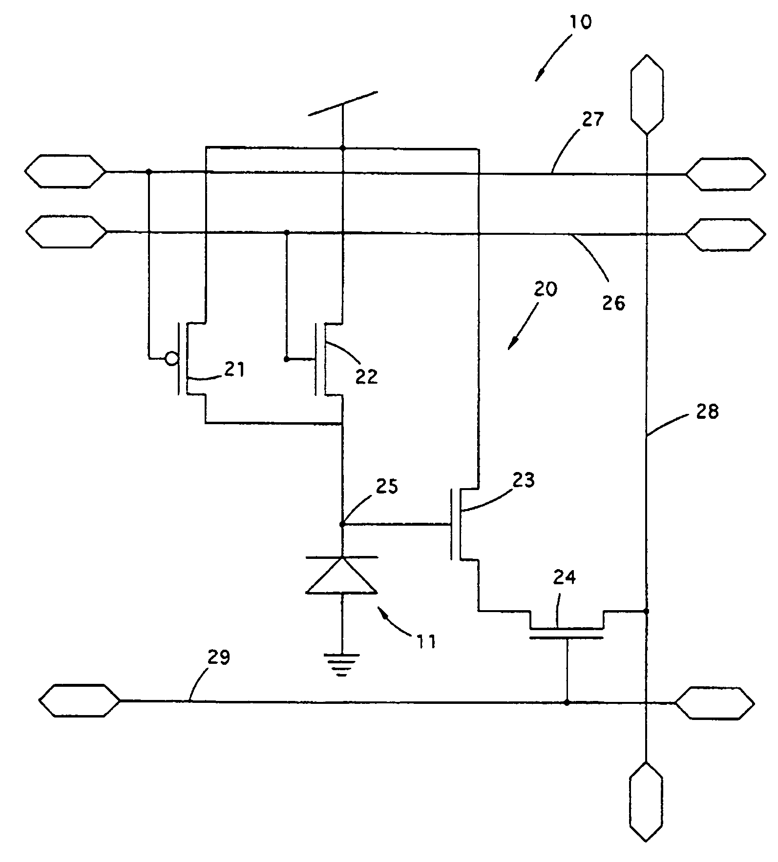
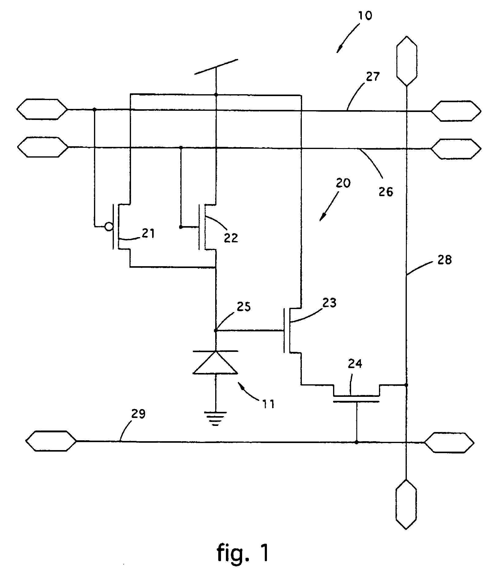
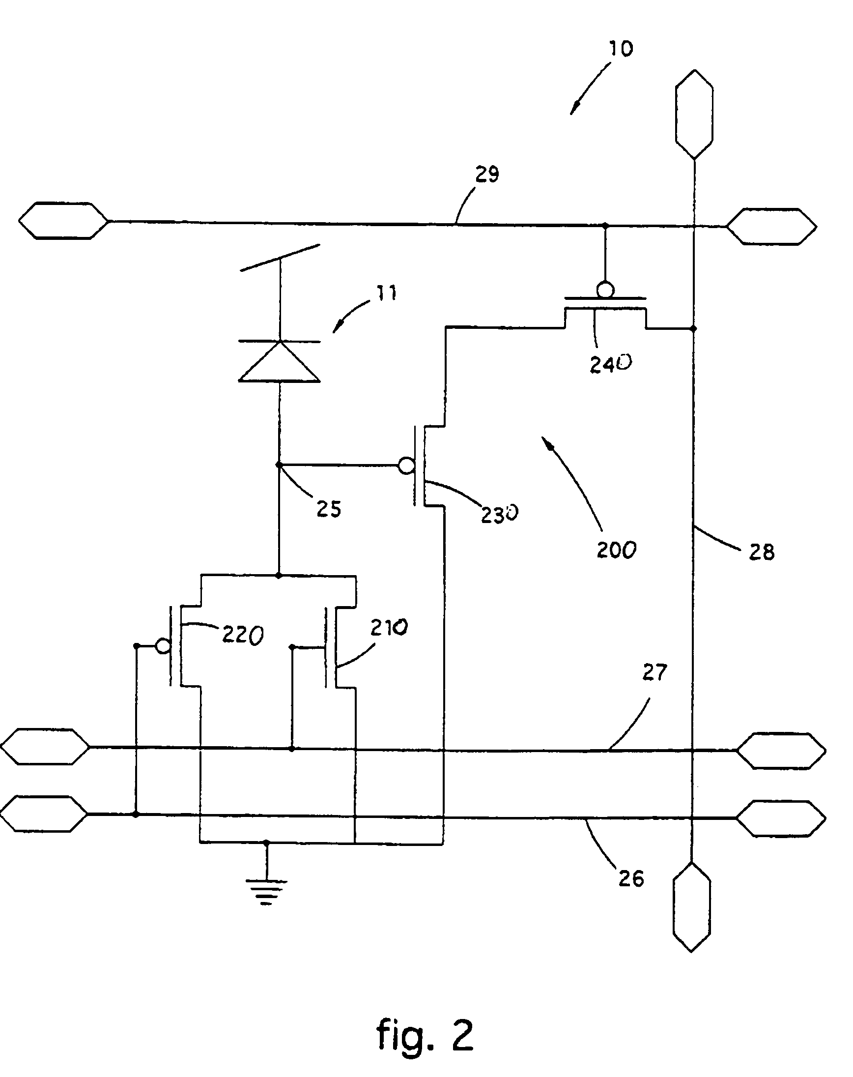
[0038]With reference to the attached drawings, and particularly to FIG. 1, a photo-sensitive element or pixel 10 according to the present invention consists of an inversely polarized diode 11 defining a photosensitive node 25, two transistors, respectively a first 21 of the P-channel type and a second 22, of the N-channel type, to polarize the photo-diode, and an amplification and reading circuit 20 comprising two transistors, respectively third 23 and fourth 24.

[0039]In the preferential embodiment, the first 21 and the second 22 transistors are of the CMOS type. When the first transistor 21 is of the P-channel type, it is able to represent an ideal switch, and when the second transistor 22 is of the N-channel type it is able to represent an active load. The number of N-channel type transistors may vary from 1 to 12 in order to increase by a corresponding value the logarithmic conversion gain of the current photo-generated by the polarized diode 11. The pixel 10 is of the type able ...


PUM


Abstract

A photo-sensitive element for electro-optical sensors, includes a photo-sensitive reception member, a current conversion circuit to convert the current generated by the photo-sensitive reception member into a voltage signal, and an amplification and reading circuit. The current conversion circuit includes a P-channel transistor used as an ideal key and piloted with a voltage that can vary between a high feed voltage and a low feed voltage. The photo-sensitive element is taken to a reset state if the pilot voltage of the transistor is low, and to an integration state if the pilot voltage is high.

Description

FIELD OF THE INVENTION[0001]The present invention concerns a photo-sensitive element used in electro-optical sensors, suitable to detect an incident light and to convert it into a correlated electric signal.[0002]The photo-sensitive element according to the present invention is used to make electro-optical sensors of a two-dimensional matrix or linear type, which can be used in various electronic devices for artificial vision, such as for example digital video cameras, smart optical sensors or otherwise.[0003]The photo-sensitive element according to the invention guarantees a very satisfactory image quality both in conditions of low light and also in the presence of uncontrolled light, hence characterized by variable intensity over a wide interval, for example to make electro-optical sensors used in the field of automotive, in security controls, in road safety control and in traffic control.BACKGROUND OF THE INVENTION[0004]Optical sensors are known, consisting of a plurality of phot...

Claims


Application Information

Patent Timeline
Patent Type & Authority Patents(United States)
IPC IPC(8): G01J1/44H04N5/355H04N5/3745
CPCH04N5/35518H04N5/3745H04N25/573H04N25/77
Inventor SARTORI, ALVISEVATTERONI, MONICA
Owner ETH LAB SRL
Why Eureka
Try Eureka