Light-receiving method of an avalanche photodiode and a bias control circuit of the same
a technology of avalanche photodiodes and control circuits, which is applied in the direction of photometry using electric radiation detectors, optical radiation measurement, instruments, etc., can solve the problems of increasing the noise involved in the photo current output of the apd, the complexity of the preparation of the pin-pd independently on the apd, and the insufficient presetting of the apd optical sensitivity, etc., to achieve the effect of small temperature dependen
- Summary
- Abstract
- Description
- Claims
- Application Information
AI Technical Summary
Benefits of technology
Problems solved by technology
Method used
Image

Examples
first embodiment
[0025] (First Embodiment)
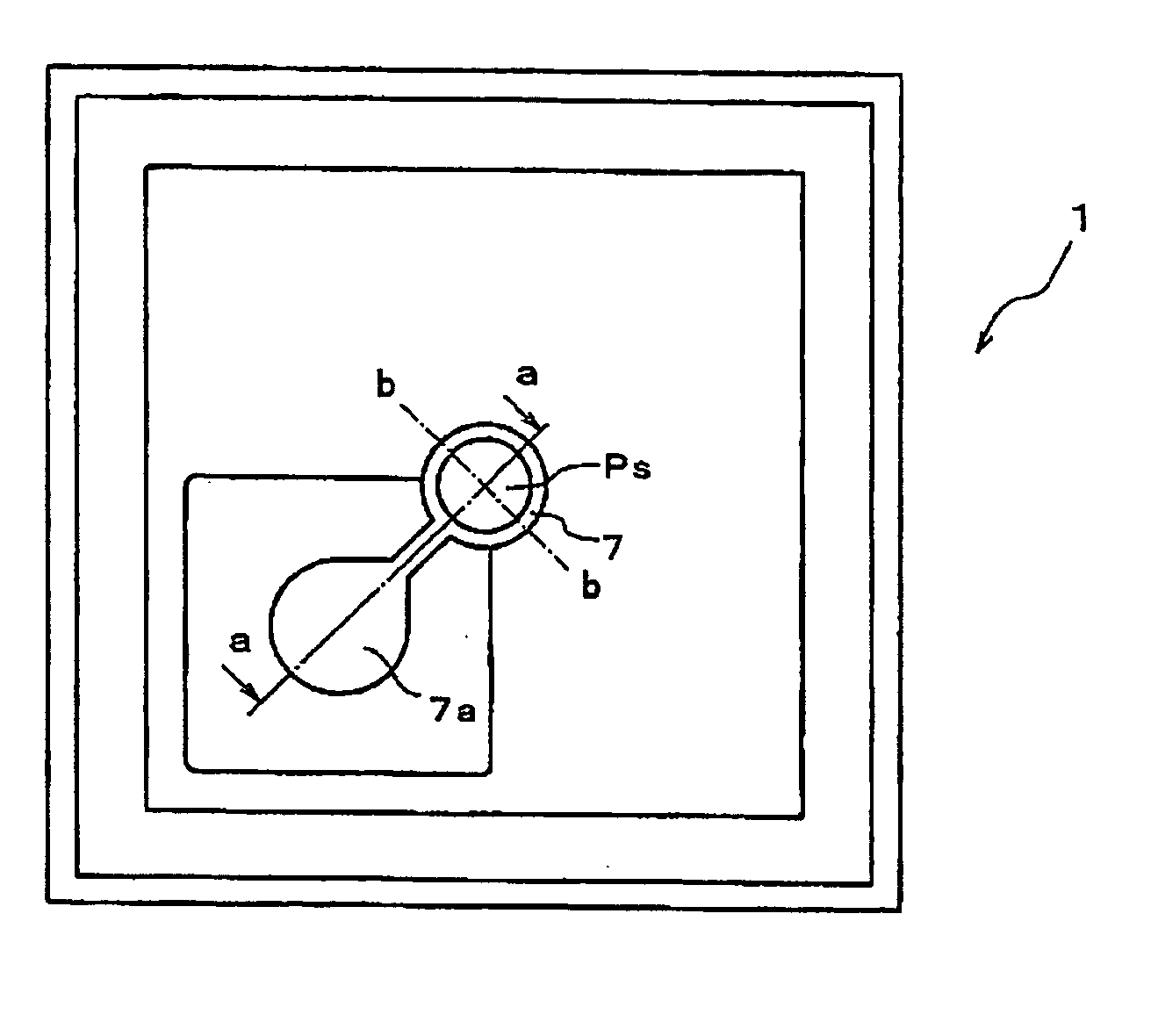
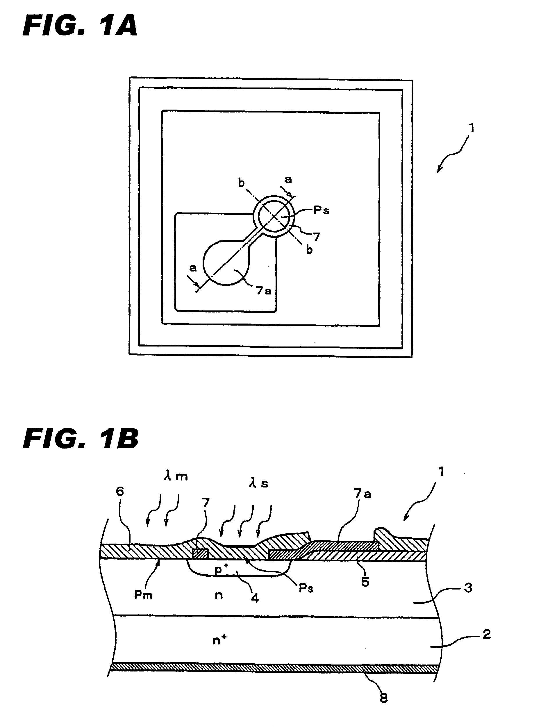
[0026] Next, preferred embodiments of the present invention will be described as referring to accompanying drawings. FIG. 1A and FIG. 1B are a plan and a sectional view, respectively, they are showing an avalanche photodiode (APD) used in the present invention. The APD 1 includes a heavily doped substrate 2, an n-type active layer 3, a heavily doped p-type diffusion layer 4, an insulating film 6, a p-electrode 7 with a pad 7A, and an n-electrode 8. Further, the APD includes a first sensitivity region PS and a second sensitivity region PM on a primary surface thereof.
[0027] As shown in FIG. 1A, the first region PS, which has a multiplication function, is formed in a restricted center region of the surface. The p-electrode 7 formed to surround the first region PS, extracts the pad 7A to which a bias voltage for the PD to be supplied between the n-electrode 8 provided in a whole surface of the back surface of the APD 1. The APD 1 is formed such that (1) the ac...
second embodiment
[0039] (Second Embodiment)
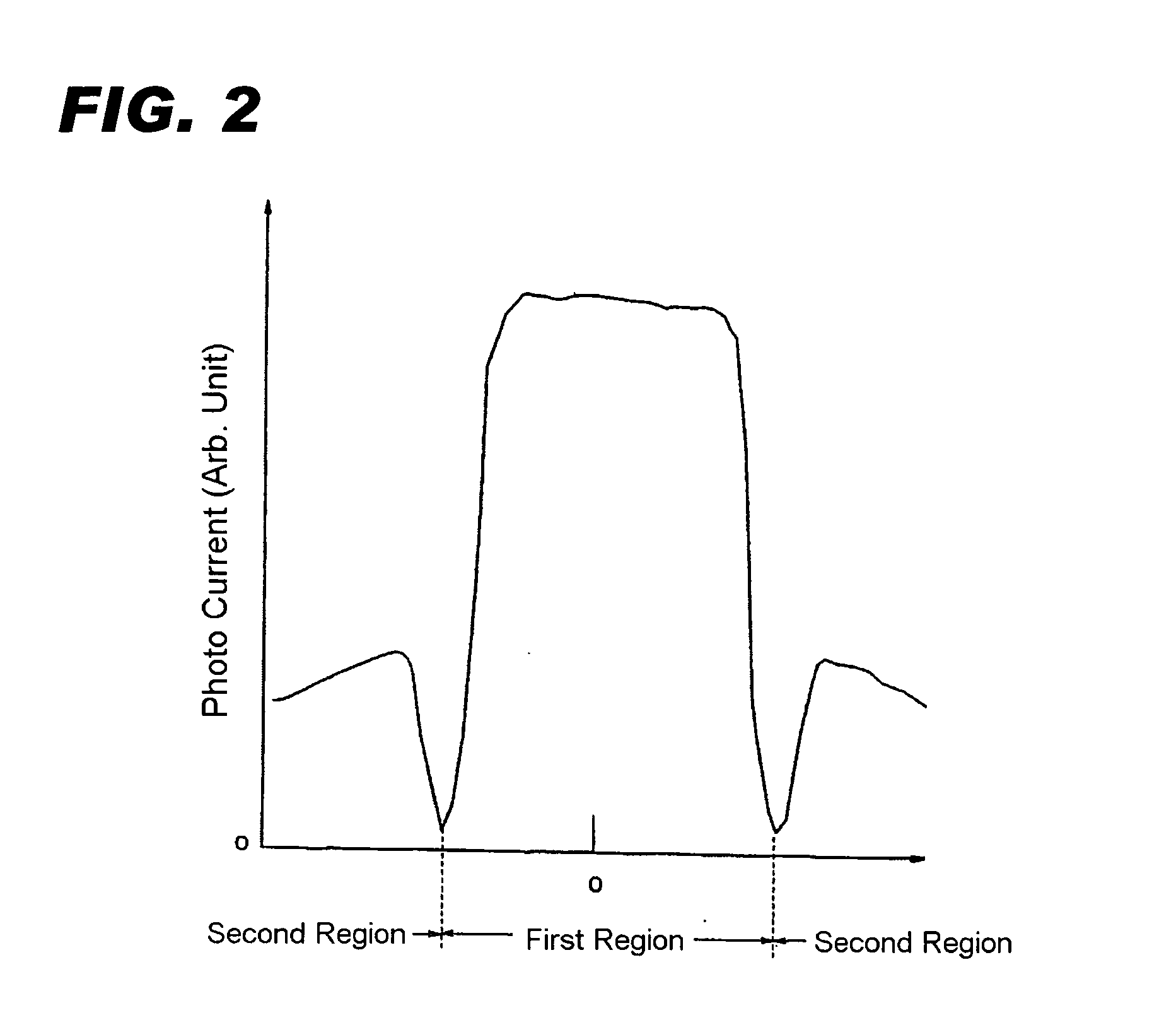
[0040] The bias voltage for the APD is 10 conventionally configured such that, when the optical input becomes large, the multiplication factor may automatically decrease and reduce the bias current. However, the circuit shown in FIG. 4 controls the bias voltage to the APD 10 such that the first signal containing the IS and INO is equal to the monitor signal IM multiplied by the gain G. The magnitude of the light detected at the first region PS is proportional to that detected at the second region PM. as far as the beam spot, the shape and the location on the APD 10, does not change. Therefore, the increase of the signal IS corresponding to the light detected by the first region means that the signal IM corresponding to the light detected by the second region becomes large. Therefore, the APD 10 may be broken by the photo current generated by it self at the condition that a large optical enters. Further, when the photo current generated by the APD 10 becomes...
PUM
 Abstract
Description
Claims
Application Information
 - R&D Engineer
- R&D Manager
- IP Professional
- Industry Leading Data Capabilities
- Powerful AI technology
- Patent DNA Extraction
Browse by: Latest US Patents, China's latest patents, Technical Efficacy Thesaurus, Application Domain, Technology Topic.
© 2024 PatSnap. All rights reserved.Legal|Privacy policy|Modern Slavery Act Transparency Statement|Sitemap