Quantum nanostructure semiconductor laser

Inactive Publication Date: 2006-03-09
NAT INST OF ADVANCED IND SCI & TECH
View PDF7 Cites 10 Cited by
  • Summary
  • Abstract
  • Description
  • Claims
  • Application Information

AI Technical Summary

Benefits of technology

[0029] The quantum nanostructure semiconductor laser according to any of the above configurations can also be used as the light source of a diffuse optical tomography apparatus. In accordance with this invention, high-density vertically and horizontally stacked multiple finite-length quantum wires or quantum dots can be formed at a desired location in the device structure of a quantum nanostructure semiconductor laser by a one-time selective growth procedure, in addition to which an optical waveguide structure required for a semiconductor laser or modulator can be realized with a very simple manufacturing process.
[0030] Moreover, since it does not have a separately-formed buried structure (the optical waveguide having a peripheral sidewall that is at least as high as the height of the active region and is exposed or covered only by an insulation layer), problems such as current leakage from the buried semiconductor (conductive) layer used in the conventional structure essentially do not arise, and there is also no thyristor effect caused by the carrier injection conditions. There is therefore no need to take the kind of countermeasures that are required in the prior art structures to deal with such problems. Parasitic capacitance is also low, making the device suitable for high-speed operation.
[0031] It also becomes easy to fabricate more advanced quantum nanostructure semiconductor lasers such as dispersion-compensated mode-locked lasers, using chirped quantum wire arrays, and significant application to wavelength division multiplexing laser arrays for optical multiplex communications, semiconductor optical modulators and various other optical functional devices can be expected.
[0032] Looking

Problems solved by technology

However, the use of multiple lithography and crystal growth steps steeply increased the manufacturing cost, preventing it becoming widespread on an industrial scale.
Thus, fundamentally there were limits to the technique, making it inapplicable, without modification, on a continuing basis into the future.
It is possible to use a ridge substrate to form a buried heterostructure such as is disclosed in Reference 6, but it is difficult to suppress current feeding through the current blocking layers due to the thyristor effect.
However, the techniques dis

Method used


Image

  • Quantum nanostructure semiconductor laser
  • Quantum nanostructure semiconductor laser
  • Quantum nanostructure semiconductor laser

Examples


Embodiment Construction

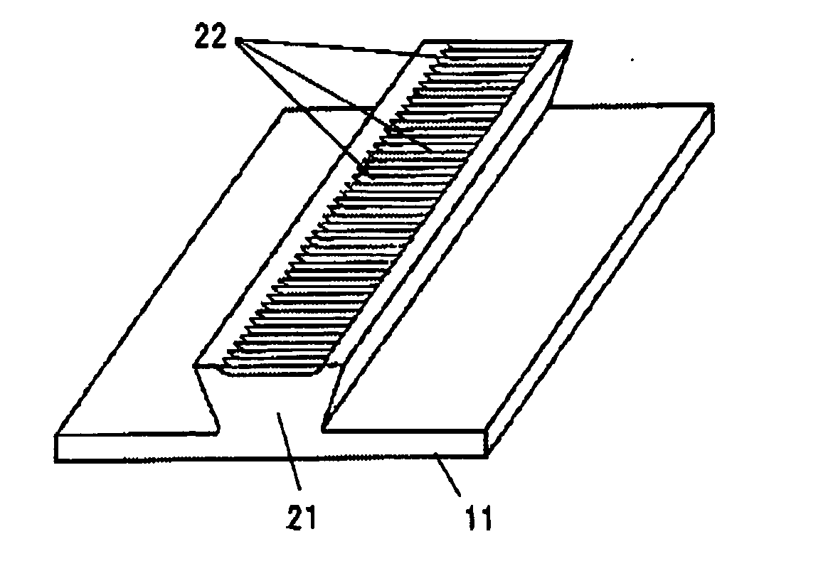
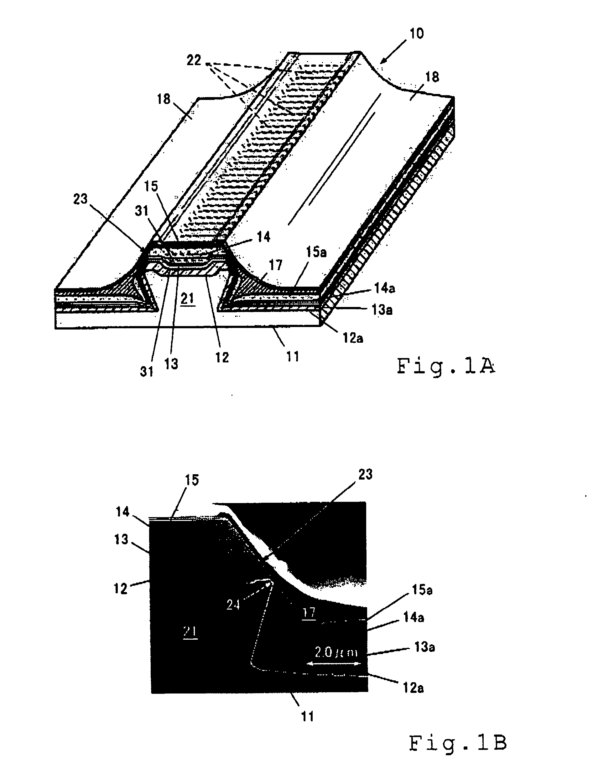
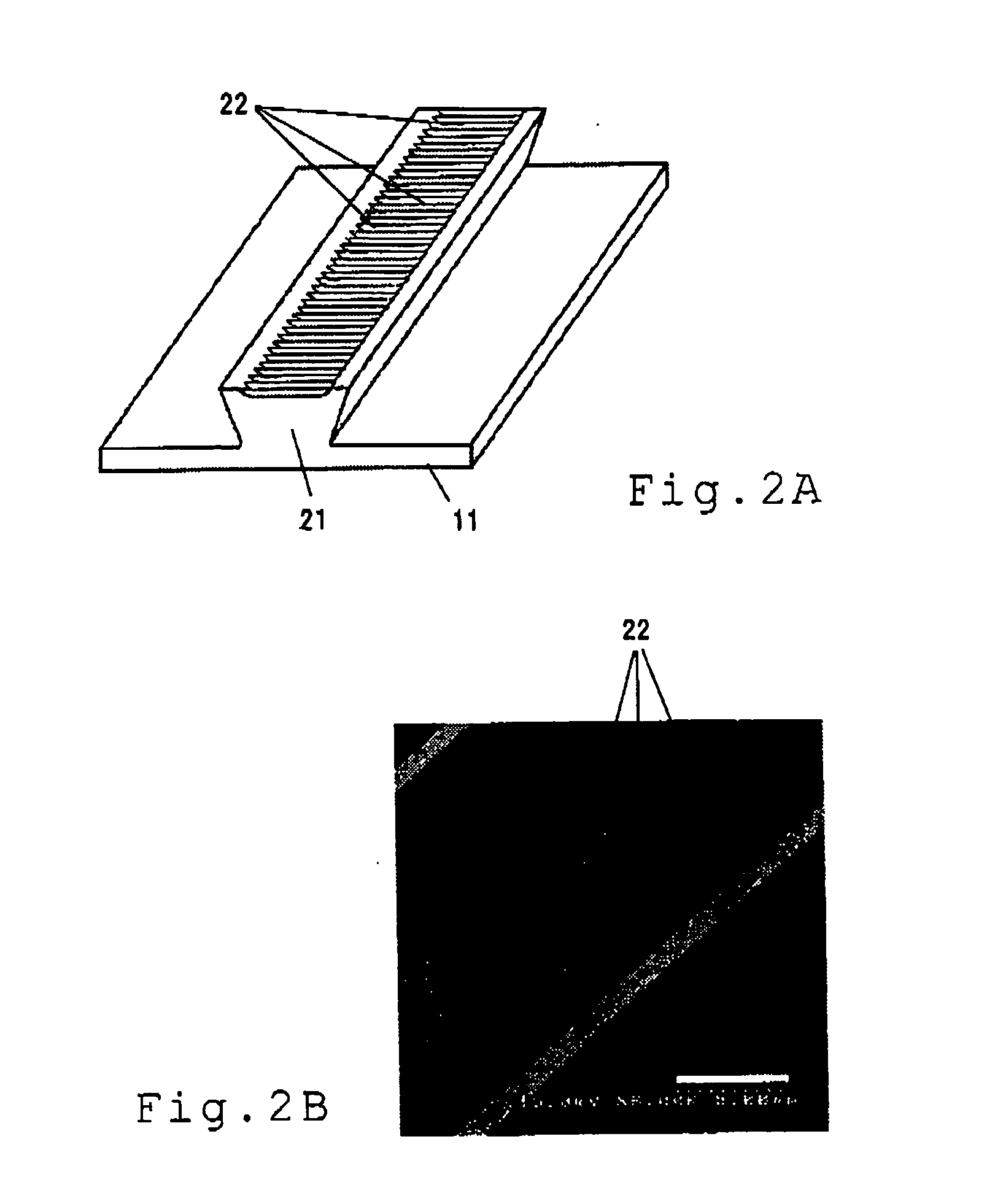
[0052]FIG. 1A shows the structure of a quantum nanostructure semiconductor laser that is a first preferred embodiment of the present invention, and FIG. 1B is a scanning electron micrograph showing an enlarged view of the principal portions. A compound semiconductor substrate 11 provides the overall physical and mechanical support for the device. A ridge 21 is formed on the substrate 11. The ridge 21 is formed as a stripe extending along the direction of laser beam emission, and preferably has a reverse mesa shape. A plurality of parallel V-grooves 22 is formed on the surface of the ridge 21, with each of the V-grooves 22 extending orthogonally to the lengthwise direction of the ridge 21.

[0053] A technique that is already known, such as from Reference 4, is used to epitaxially grow at least a lower cladding layer 12 on the ridge 21, which is followed by the forming of finite length quantum wires 13 at a position corresponding to the position of the V-grooves 22, an upper cladding l...


PUM


Abstract

A quantum nanostructure semiconductor laser is provided that does not use a buried structure defined by etching and regrowth processes in the prior arts, and can be manufactured using a procedure that is simple and has good reproducibility. This helps to reduce the threshold current and provides good lasing wavelength stability. The laser has a stripe-shaped ridge with a plurality of V-grooves formed on a compound semiconductor substrate in the direction of laser beam emisson, with the V-grooves being arrayed in parallel, with each V-groove extending orthogonally to the direction of laser beam emission. On the ridge, an optical waveguide is provided that comprises a lower cladding layer, a plurality of quantum wires and an upper cladding layer formed in order by a crystal growth process. The quantum wires are formed to a finite length corresponding to the stripe width of the laser beam, and are each located at a position corresponding to a V-groove, thereby constituting the laser active region. The optical waveguide is trapezoidal in shape, and has a peripheral sidewall that is at least as high as a height at which the quantum wires are located, and is exposed or covered only by an insulation layer.

Description

BACKGROUND OF INVENTION [0001] 1. Field of the Invention [0002] The present invention relates to an improved quantum nanostructure semiconductor laser that is particularly suited for application to distributed feedback (DFB) semiconductor lasers. [0003] 2. Description of the Prior Art [0004] Distributed feedback semiconductor lasers provided with a periodic gain or refractive index structure along the waveguide, are important in future wavelength multiplex communication systems due to the fact that it is possible to closely control their lasing wavelength and that they can readily be integrated since, unlike in the case of a Fabry-Perot laser, they do not require a cleaving step. [0005] For future progress, the manufacturing process has to be simplified. In the conventional fabrication techniques, as described for example in “MOCVD regrowth over GaAs / AlGaAs gratings for high power long-lived InGaAs / AlGaAs lasers,” P. K. York, J. C. Connolly, et al., Journal of Crystal Growth 124 (19...

Claims


Application Information

Patent Timeline
IPC IPC(8): H01S5/00H01S5/12
CPCB82Y10/00B82Y20/00H01S5/02284H01S5/0265H01S5/12H01S5/1231H01S5/4087H01S5/2201H01S5/2213H01S5/341H01S5/34313H01S5/4031H01S5/22H01S5/02251
Inventor OGURA, MUTSUO
Owner NAT INST OF ADVANCED IND SCI & TECH
Why Eureka
Try Eureka