Semiconductor acceleration sensor

a technology of acceleration sensor and semiconductor, applied in the direction of speed/acceleration/shock measurement, force measurement, instruments, etc., can solve the problems of high manufacturing cost, high cost, irregular delivery time, etc., and achieve the effect of reducing offset voltage, excellent sensitivity, and low temperature dependence of offset voltag

Inactive Publication Date: 2006-03-30
HITACHI METALS LTD
View PDF1 Cites 12 Cited by
  • Summary
  • Abstract
  • Description
  • Claims
  • Application Information

AI Technical Summary

Benefits of technology

[0011] An object of the invention is to provide a cheap and highly sensitive semiconductor acceleration sensor that enhances X-axis and Y-axis outputs without reducing Z-axis output and does not need to prepare amplifiers different in amplitude for each axis.
[0020] In the semiconductor acceleration sensor of the invention, each of the flexible arms supporting the mass portion has in the center the narrower portion that is smaller in cross section area than the wider portions positioned at the ends of the flexible arm so that the mass portion is easily moved by an applied acceleration and that the flexible arms extending in a direction of the applied acceleration can be bent largely. By the reason, detection sensitivity of the acceleration sensor increases for acceleration in each axial direction in the top surface of the mass portion, that is, an extending direction of the flexible arm.
[0021] For example, when acceleration is applied to an acceleration sensor in X-axis direction, flexible arms (Y-axis direction) extending vertical to the acceleration prevent a mass portion from displacing in X-axis direction. But, the interference by the vertical flexible arms is reduced in the acceleration sensor of the invention since the Y-axis flexible arms have a narrower portion. It is considered that a detection sensitivity in X-axis direction is enhanced by the reason.
[0022] When both flexible arms of X-axis direction and those of Y-axis direction are provided with the narrower portions on them, both detection sensitivity in Y-axis direction and that in X-axis direction are increased. As a result, detection sensitivities in X-axis direction and Y-axis direction can be made on the same level with that in Z-axis direction.
[0027] Since the piezo resistors are provided restrictedly within a region of the top surface of the wider portions of the flexible arm from a boundary between the flexible arm and the mass portion or the support frame, the piezo resistors are positioned at a position that has the largest deformation on the flexible arm by acceleration and show excellent sensitivity. Also, since there is on the flexible arm no through-hole connecting a piezo resistor to a metal wire, the piezo resistor shows a reduced offset voltage, and a temperature dependency of the offset voltage is very small.
[0028] As discussed above, in the semiconductor acceleration sensor, acceleration detection sensitivity in each direction in the top surface of the mass portion, that is, X-axis direction and Y-axis direction, is enhanced to make the sensitivity on a level with acceleration detection sensitivity in a direction, Z-axis direction, vertical to the top surface of the mass portion. Further, the acceleration detection sensitivities are made higher than a conventional one but also the offset voltage becomes smaller and the temperature dependency of the offset voltage becomes smaller.

Problems solved by technology

However, the thickness of Si single crystal substrates used for semiconductors and the like is mainly set at 625 μm and 525 μm, and thus Si single crystal substrates of about 800 μm have to be specially ordered, resulting in irregular delivery times as well as high cost.
At least several impurity implanting steps are necessary to change the concentration of impurity elements, resulting in higher manufacturing cost and lower equipment capacity.
Thus, this method is not preferable.
Moreover, the conventional acceleration sensor is configured such that the output of the Z axis is larger than that of the X axis, resulting in a large output difference between the axes.

Method used


Image

  • Semiconductor acceleration sensor
  • Semiconductor acceleration sensor
  • Semiconductor acceleration sensor

Examples


example 1

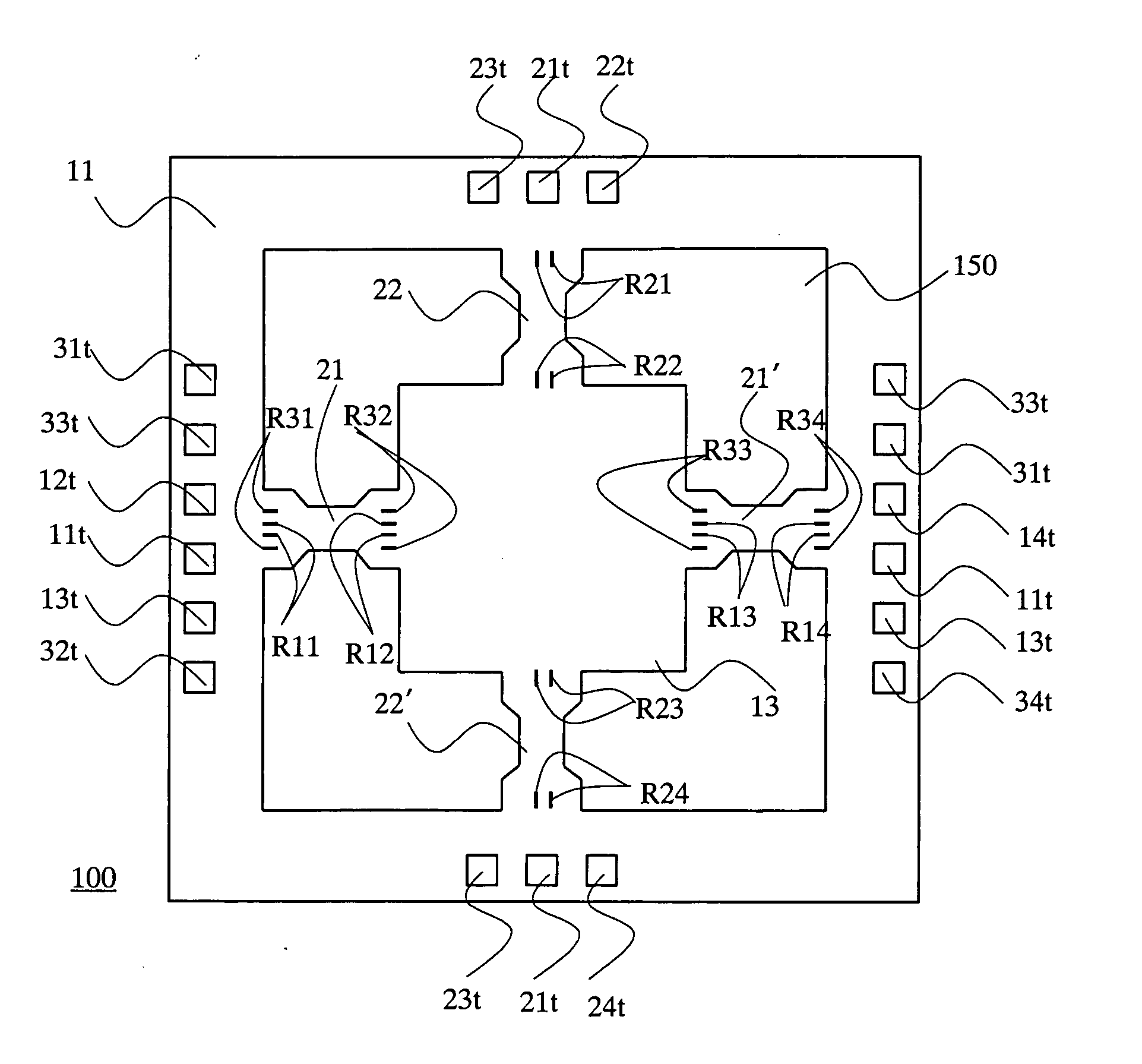
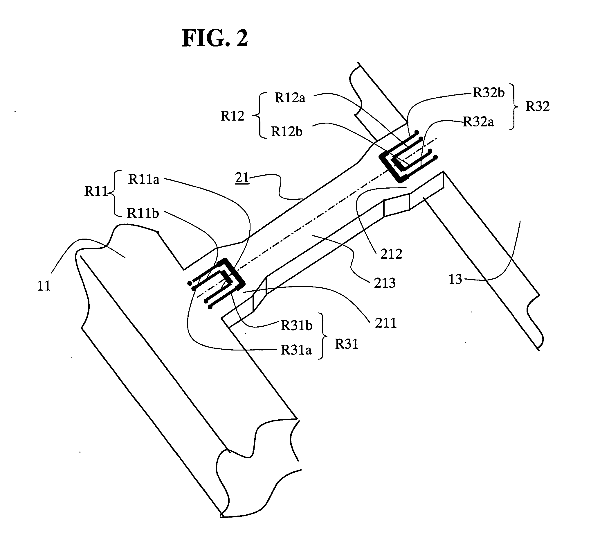
[0046] Referring to FIGS. 1 through 5, a semiconductor acceleration sensor of the invention will be described below. FIG. 1 is a plan view showing the semiconductor acceleration sensor. FIG. 2 is a perspective view showing the enlargement of a flexible arm of the semiconductor acceleration sensor. In FIGS. 1 and 2, metal wires are omitted.

[0047] The semiconductor acceleration sensor of the invention is made up of a silicon single crystal substrate where an SOI layer is formed through an SiO2 insulating layer to accurately control the thickness of the flexible arm, that is, an SOI wafer. SOI is an abbreviation of Silicon On Insulator. In this example, a thin SiO2 insulating layer (about 1 μm) serving as an etching stopper is formed on an Si wafer having a thickness of about 625 μm. A wafer having an N-type silicon single crystal layer with a thickness of about 10 μm is used as a substrate on the insulating layer. In a semiconductor acceleration sensor 100 of this example, four L-sha...

example 2

[0072] According to the semiconductor acceleration sensor of Example 1, acceleration sensors were manufactured in which the narrower portions of flexible arms (700 μm in length) are changed in length from 200 μm to 400 μm, and sensitivity ratios (Ex / Ez) were evaluated. The flexible arms had an even thickness of 5 μm, and the dimensions of a piezo resistor, the dimensions of a metal wire, and the thickness of a silicon oxide insulating layer were the same as the acceleration sensor of Example 1. A wider portion was 110 μm in width, the narrower portion was 52.5 μm in width, and a cross section area ratio (b / a) of a cross section area (b) of the wider portion to a cross section area (a) of the narrower portion was 2.1.

[0073] Twenty acceleration sensors were prepared in which narrower portions were changed in length from 200 μm to 400 μm. The acceleration sensors were placed in the protection case shown in FIG. 15. The bottom of a support frame was fixed on a bottom plate in the prote...

example 3

[0074] A semiconductor acceleration sensor of Example 3 has a flexible arm different in shape from Example 1. As shown in the perspective view of FIG. 8, in the flexible arm of the semiconductor acceleration sensor according to Example 3, wider portions 211′ and 212′ and a narrower portion 213′ have an equal width of 110 μm. The narrower portion 213′ is thinner than the wider portions 211′ and 212′. The wider portion was 8 μm in thickness and the thickness of the narrower portion was changed from 1.74 μm to 8 μm.

[0075] Twenty acceleration sensors were manufactured in which a cross section area ratio (b / a) of a cross section area (b) of the wider portion to a cross section area (a) of the narrower portion was changed from 1 to 4.6, and the sensitivity and the impact resistance were evaluated. The acceleration sensors were placed in a protection case shown in FIG. 15. The bottom of a support frame was fixed on a bottom plate in the protection case with adhesive and a clearance betwee...


PUM


Abstract

A semiconductor acceleration sensor is disclosed which has a small difference in acceleration detection sensitivity among X, Y, and Z axes and a high detection sensitivity. The acceleration sensor has a mass portion in its center, a support frame surrounding the mass portion, and a plurality of flexible arms connecting the mass portion and the support frame. The flexible arm has wider portions on both ends and a narrower portion between the wider portions. Piezo resistors are restrictedly provided within a top surface region of the wider portion of the flexible arm, and through holes connecting metal wires and the piezo resistors are disposed on the mass portion / support frame. The plurality of flexible arms are symmetric with respect to the center of the mass portion, and each of the flexible arms is symmetric with respect to the center line of the flexible arm.

Description

BACKGROUND OF THE INVENTION [0001] b 1. Field of the Invention [0002] The invention relates to a semiconductor acceleration sensor which is used for a portable terminal equipment, a toy, an automobile, an aircraft and the like to detect an acceleration. [0003] 2. Description of the Related Art [0004] The following will discuss the configuration of a conventional three-axis acceleration sensor using piezo resistors. FIG. 15 is an exploded perspective view showing the acceleration sensor. In such an acceleration sensor, an acceleration sensor element 200 is fixed on a case 2 with adhesive and a lid 3 is fixed on the protection case 2 with adhesive. External terminals 7 of the acceleration sensor element 200 and terminals 5 of the protection case 2 are connected via metal wires 4. The output of the acceleration sensor element 200 is drawn from external terminals 6 of the protection case 2 to the outside. In this specification, the acceleration sensor element 200 will be referred to as ...

Claims


Application Information

Patent Timeline
Patent Type & Authority Applications(United States)
IPC IPC(8): G01P15/09G01P15/12G01P15/18
CPCG01P15/0802G01P15/18G01P15/123G01P15/09
Inventor IKEDA, YOSHIOHOSODA, MASAYUKISAKAGUCHI, ISAOSAITOH, MASAKATSU
Owner HITACHI METALS LTD
Why Eureka
Try Eureka