Sonos device and methods of manufacturing the same

a semiconductor device and semiconductor technology, applied in semiconductor devices, transistors, instruments, etc., can solve problems such as the increase of the potential for misalignment of the ono layer, and achieve the effect of increasing program and erasing efficiency

Active Publication Date: 2005-05-05
SAMSUNG ELECTRONICS CO LTD
View PDF3 Cites 9 Cited by
  • Summary
  • Abstract
  • Description
  • Claims
  • Application Information

AI Technical Summary

Benefits of technology

[0014] Exemplary embodiments of the present invention provide silicon-oxide-nitride-oxide-silicon (SONOS) devices that can increase program and erase efficiency and form a uniform charge trapping layer among different cells, and methods of manufacturing the same.

Problems solved by technology

Consequently, the potential for misalignment of the ONO layer increases.

Method used


Image

  • Sonos device and methods of manufacturing the same
  • Sonos device and methods of manufacturing the same
  • Sonos device and methods of manufacturing the same

Examples


Embodiment Construction

[0028] Exemplary embodiments of the invention will now be described more fully with reference to the accompanying drawings.

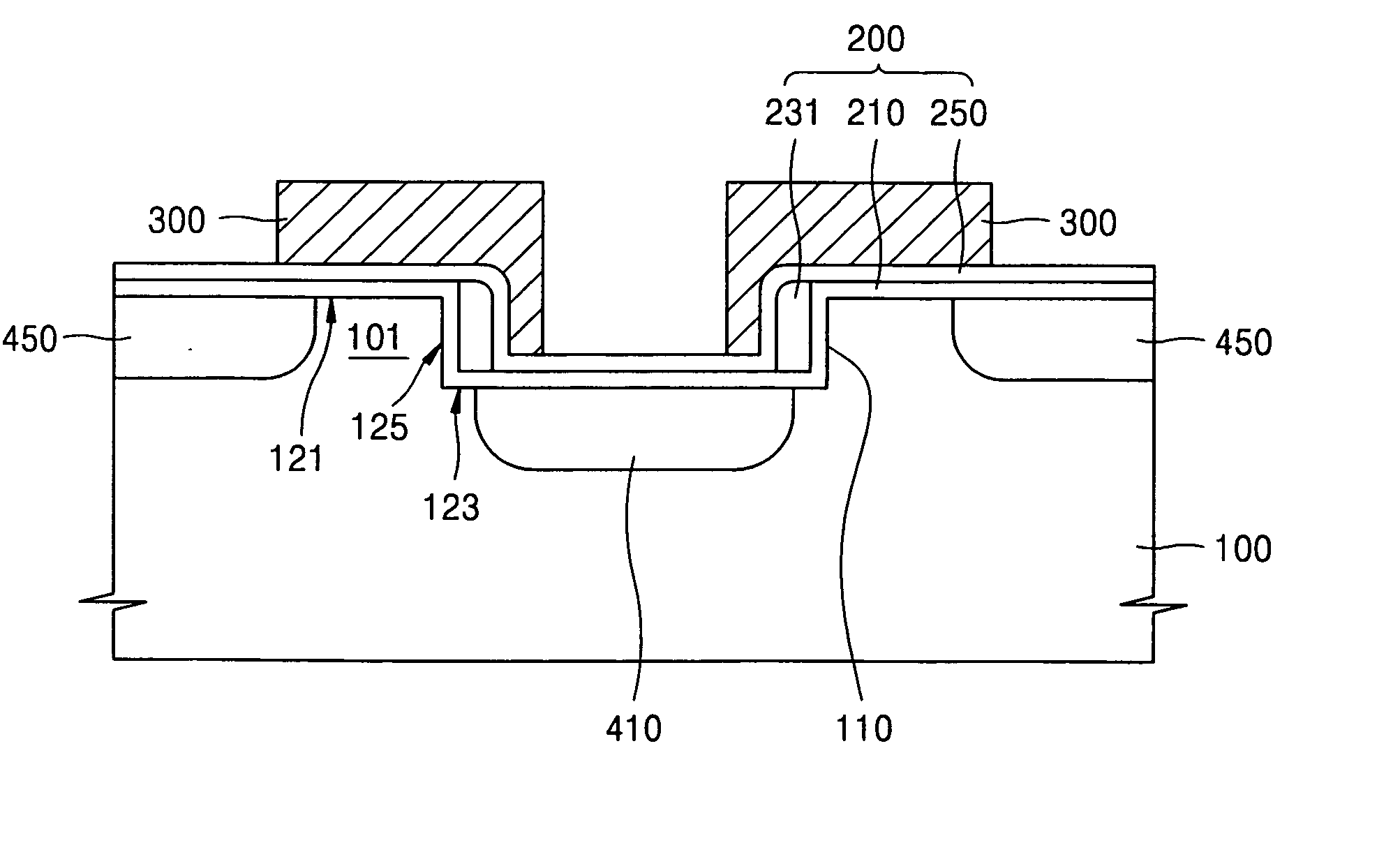
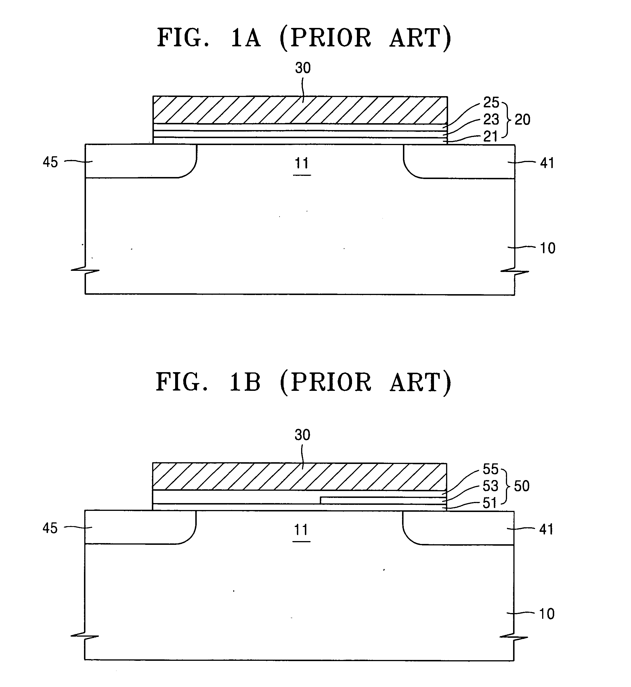
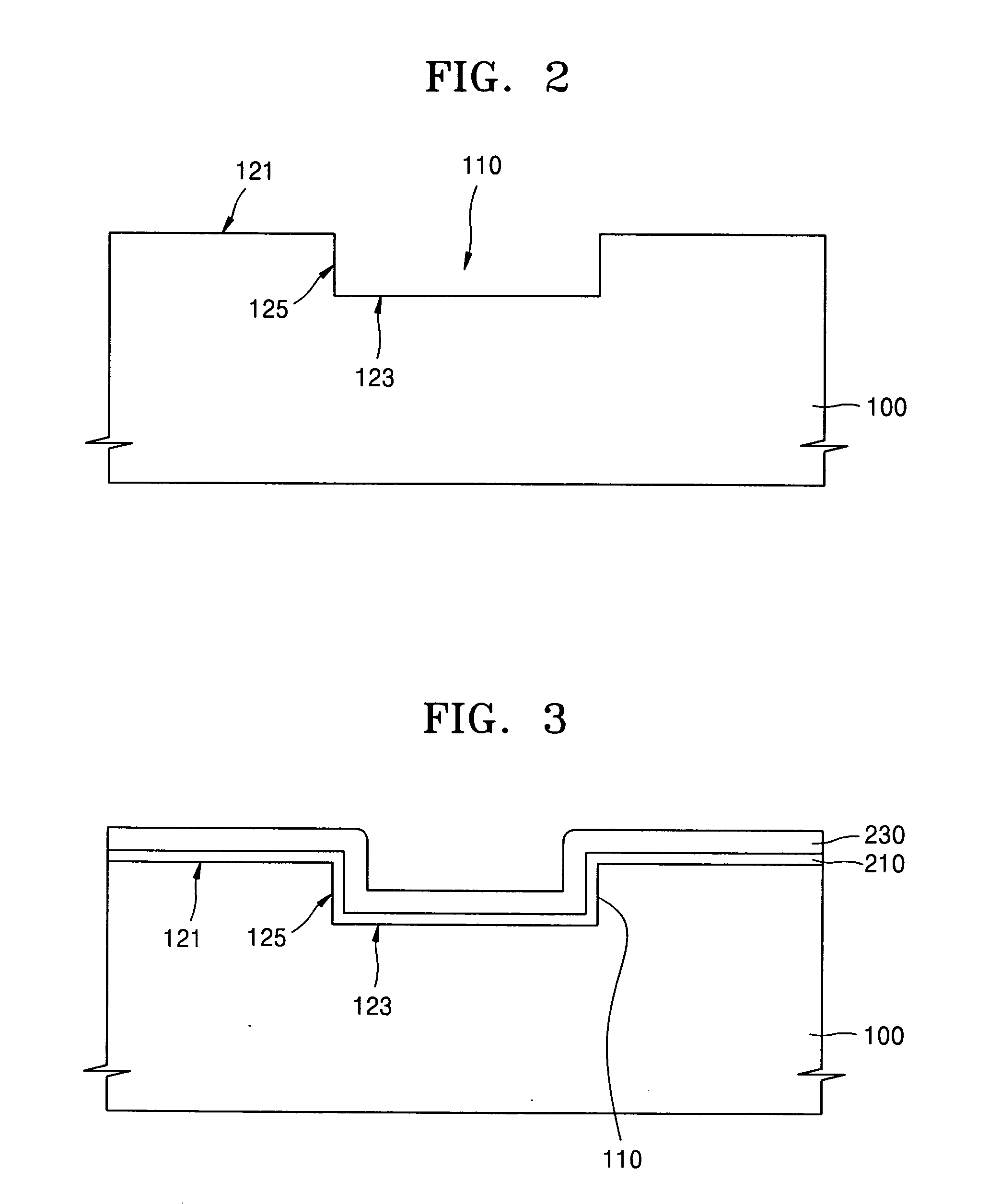
[0029] Exemplary embodiments of the present invention provide a cell structure of a local silicon-oxide-nitride-oxide-silicon (SONOS) device. According to an exemplary embodiment of the present invention, a cell structure of a SONOS device having a charge trapping layer in a form of a spacer is provided. In more detail, the cell structure of the SONOS device includes a first impurity region near a charge trapping layer; a second impurity region, which is either a drain region if the first impurity region is a source region or a source region if the first impurity region is drain region. Further, the charge trapping layer faces the second impurity region and is formed in a shape of a spacer in a trench.

[0030] To form the charge trapping layer, a semiconductor substrate has a first surface, a second surface of lower elevation than the first surface, and a third ...


PUM


Abstract

Silicon-oxide-nitride-oxide-silicon (SONOS) devices and methods of manufacturing the same are provided. According to one aspect, a SONOS device includes a semiconductor substrate having a first surface, a second surface of lower elevation than the first surface, and a third surface perpendicular and between the first and second surfaces; a tunnel dielectric layer on the semiconductor substrate; a charge trapping layer in a form of a spacer on the tunnel dielectric layer on the third surface; a charge isolation layer on the tunnel dielectric layer, which covers the charge trapping layer; a gate that extends over a portion of the first surface, over a portion of the second surface, and is adjacent to a portion of the third surface of the semiconductor substrate on the charge isolation layer; a first impurity region formed below the first surface and near the gate; and a second impurity region formed below the second surface, opposite the first impurity region.

Description

[0001] This application claims the priority to Korean Patent Application No. 2003-76211, filed on Oct. 30, 2003, the disclosure of which is incorporated herein by reference in its entirety. [0002] 1. Field of the Invention [0003] The present invention relates, generally, to a method of manufacturing a nonvolatile memory semiconductor device, and more particularly, to a silicon-oxide-nitride-oxide-silicon (SONOS) memory semiconductor device having an improved program and erase efficiency, and methods of manufacturing the same. [0004] 2. Description of the Related Art [0005] Among nonvolatile semiconductor memory devices, interest is focused on silicon-oxide-nitride-oxide-silicon (SONOS) devices. Unlike conventional stacked gate type nonvolatile memory devices with a floating gate, memory cells of SONOS devices have a charge trapping layer, for example, a silicon nitride layer, instead of the floating gate. [0006] SONOS devices are also known as metal-oxide-nitride-oxide-semiconductor...

Claims


Application Information

Patent Timeline
Patent Type & Authority Applications(United States)
IPC IPC(8): H01L21/8247G11C16/04H01L21/336H01L21/8246H01L27/115H01L29/788H01L29/792
CPCG11C16/0475H01L27/115H01L29/7926H01L29/66833H01L29/792H01L27/11568H10B69/00H10B43/30
Inventor PARK, YOUNG-SAMYOON, SEUNG-BEOM
Owner SAMSUNG ELECTRONICS CO LTD
Why Eureka
Try Eureka