

Semiconductor package capable of absorbing electromagnetic wave
- Summary
- Abstract
- Description
- Claims
- Application Information
AI Technical Summary
Benefits of technology
Problems solved by technology
Method used
Image

Examples
Embodiment Construction
[0022] Now, preferred embodiments of the present invention will be described in detail with reference to the accompanying drawings.
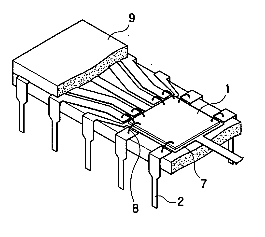
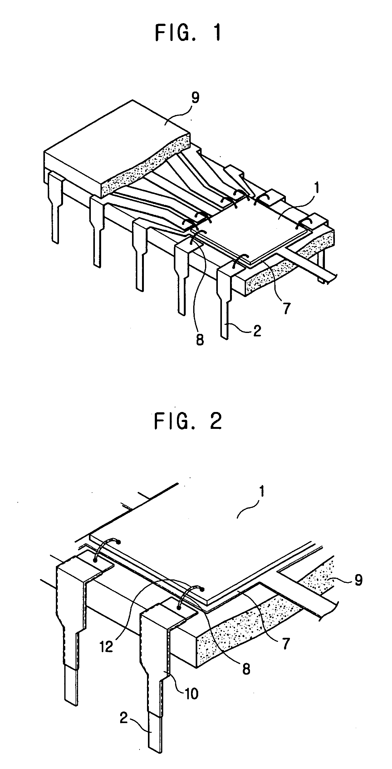
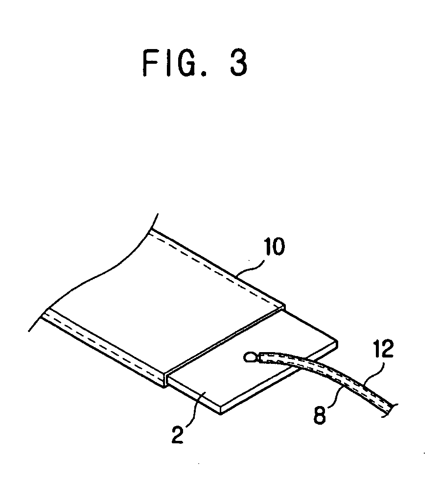
[0023]FIG. 2 is a perspective illustrating a structure for absorbing an electromagnetic wave according to the present invention, and FIG. 3 is a perspective view illustrating a detailed structure for absorbing an electromagnetic wave in a bonding wire and a conductive lead connected thereto.
[0024] Referring to FIG. 2, electromagnetic wave absorbing films 10 and 12 are uniformly coated on both or either of a conductive lead 2 and a bonding wire 8. The electromagnetic wave absorbing films 10 and 12 form a closed loop.
[0025] The electromagnetic wave absorbing films 10 and 12 are formed by coating an electromagnetic wave absorbent on predetermined portions of the conductive lead 2 and / or the bonding wire to a predetermined constant thickness and drying the coated electromagnetic wave absorbent. Here, the electromagnetic wave absorbent is made by mixing an...
PUM
 Abstract
Description
Claims
Application Information