Wireless communication nodule assembly

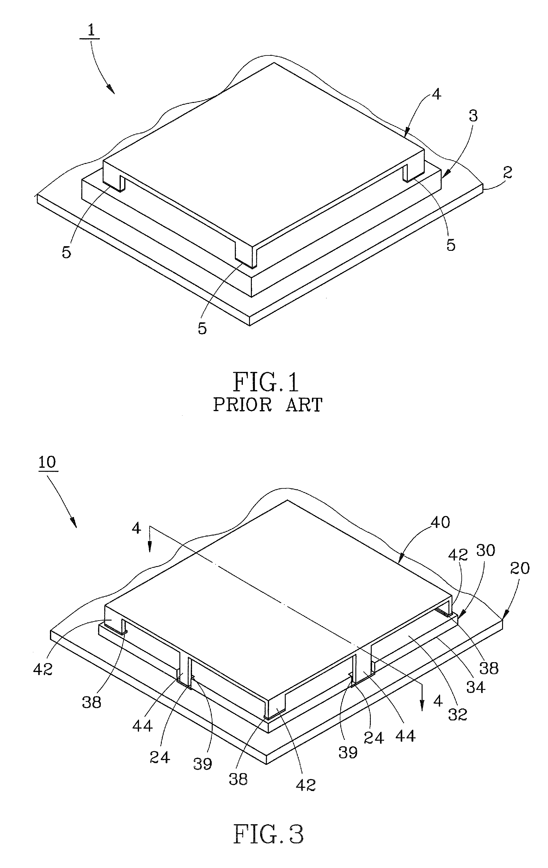
a wireless communication module and nodule technology, applied in the field of wireless communication module assembly, can solve the problems of poor grounding effect of metal cap, inability to effectively isolate electromagnetic interference (emi), drawback of conventional wireless communication module assembly b>1/b>, etc., and achieve good grounding effect and effectively minimize electromagnetic interference

Inactive Publication Date: 2008-11-27
UNIVERSAL SCI IND CO LTD
View PDF7 Cites 12 Cited by
  • Summary
  • Abstract
  • Description
  • Claims
  • Application Information

AI Technical Summary

Benefits of technology

[0007]The present invention has been accomplished in view of the above-noted circumstances. It is the primary objective of the present invention to provide a wireless communication module assembly, which can provide a good grounding effect to effectively minimize the electromagnetic interference.

Problems solved by technology

According to this design, the grounding via holes tend to produce parasitic inductance and resistance, resulting in a poor grounding effect of the metal cap.
Therefore, the wireless communication module assembly 1 cannot be well grounded to effectively isolate the electromagnetic interference (EMI).
Therefore, this design of the conventional wireless communication module assembly 1 has the drawback of poor heat-dissipative effect.

Method used


Image

  • Wireless communication nodule assembly
  • Wireless communication nodule assembly
  • Wireless communication nodule assembly

Examples


first embodiment

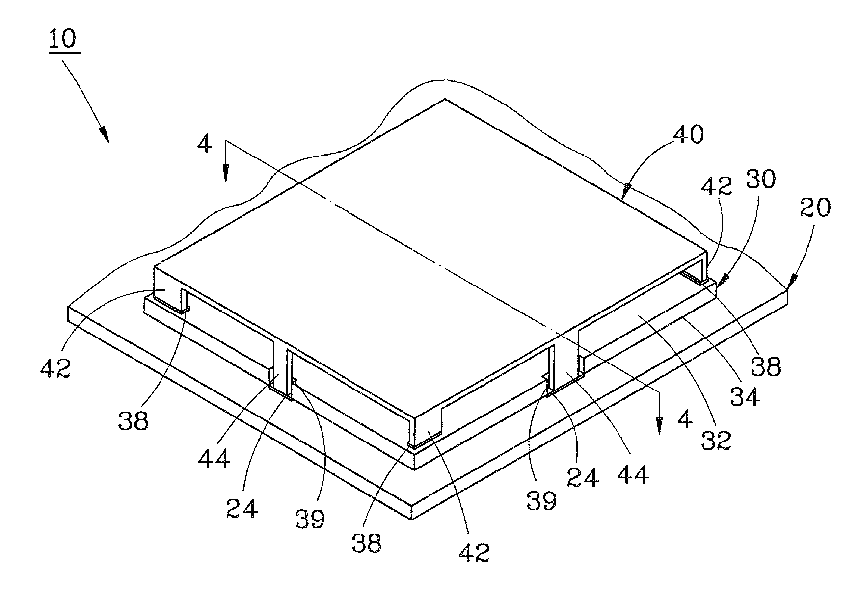
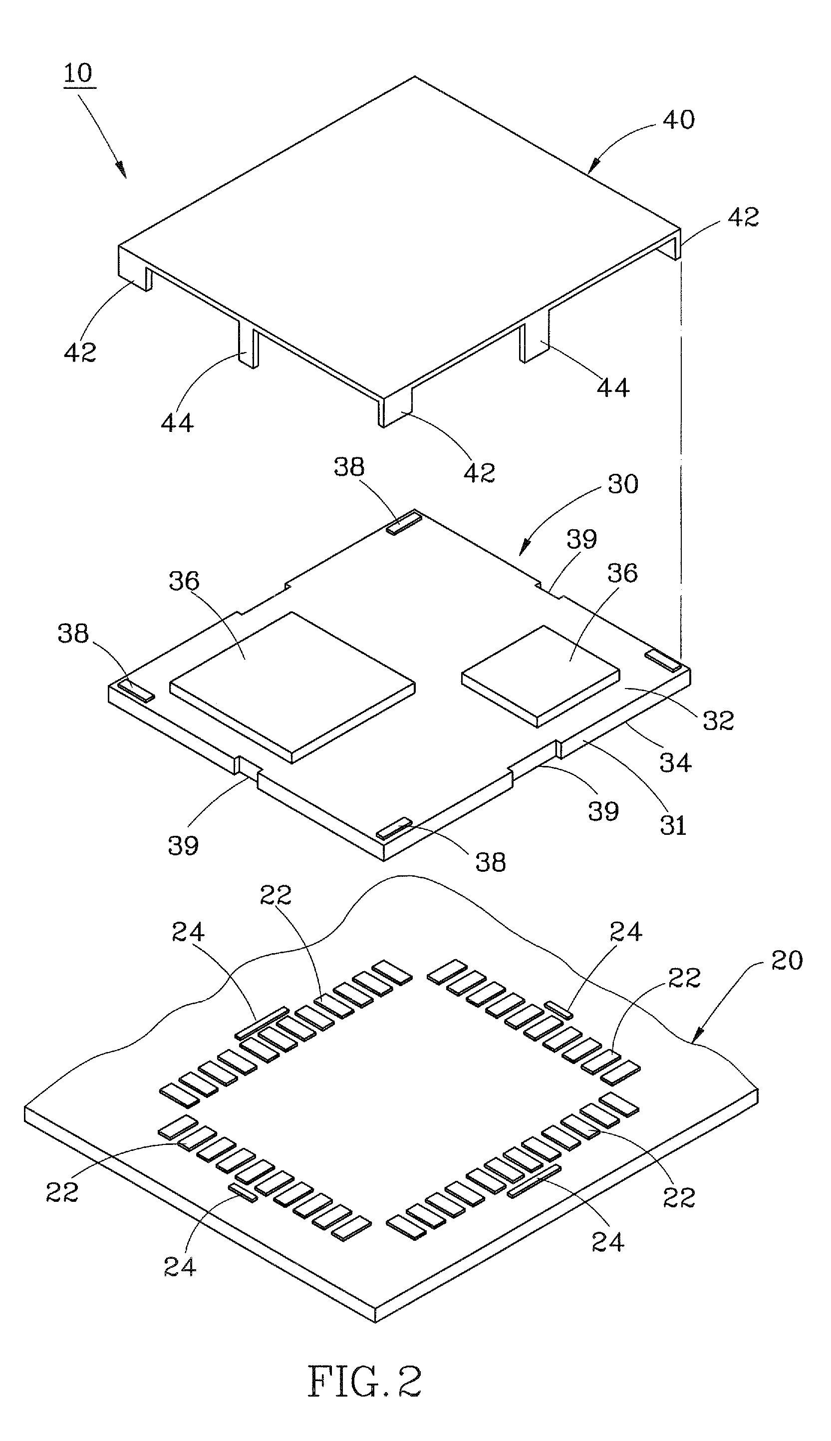
[0024]As shown in FIGS. 2-4, a wireless communication module assembly 10 in accordance with the present invention comprises a main board 20, a circuit board unit 30 including a substrate 31, and a metal cap 40.

[0025]The main board 20 has arranged a plurality of contact pads 22 and grounding pads 24 on its top surface.

[0026]The substrate 31 of the circuit board unit 30 has a top surface 32, a bottom surface 34, a plurality of contact pads 37 at the bottom surface 34, a plurality of grounding pads 38 at the top surface 32 and a plurality of notches 39 at a periphery thereof. The circuit board unit 30 further includes two chips 36 mounted on the top surface 32 of the substrate 31. It is to be easily understood that the circuit board unit 30 can be designed containing one or more chips of various functions, which can be mounted on the top surface 32 and / or the bottom surface 34 of the substrate 31, depending on the requirement of the circuit board unit 30. The contact pads 37 at the bot...

second embodiment

[0029]FIGS. 5-7 show a wireless communication module assembly 12 in accordance with the present invention. The wireless communication module assembly 12 comprises a main board 50, a circuit board unit including a spacer 60 and a substrate 70, and a metal cap 80.

[0030]The main board 50 has arranged on its top surface a plurality of contact pads 52 and a plurality of grounding pads 54.

[0031]The spacer 60 is set in between the substrate 70 and the main board 50 and electrically connected to the substrate 70 and the main board 50. The spacer 60 has a top bearing face 62, a bottom bearing face 64, a plurality of contact pads 66, and a plurality of notches 68 at a periphery thereof. The contact pads 66 of the spacer 60 are respectively arranged on the top bearing face 62 and the bottom bearing face 64. The contact pads at the top bearing face 62 are electrically connected to the contact pads at the bottom bearing face 64. The contact pads 66 at the bottom bearing face 64 are used to be el...


PUM


Abstract

A wireless communication module assembly includes a main board having a top surface on which a plurality of grounding pads are provided, a circuit board unit, and a metal cap. The circuit board unit has a bottom surface electrically mounted on the top surface of the main board, a top surface with a plurality of grounding pads, and a plurality of notches corresponding to the grounding pads of the main board. The metal cap covers the circuit board unit and has first mounting legs respectively and electrically connected with the grounding pads of the circuit board unit, and second mounting legs respectively passing through the notches of the circuit board unit and electrically connected with the grounding pads of the main board.

Description

BACKGROUND OF THE INVENTION[0001]1. Field of the Invention[0002]The present invention relates generally to a communication module and more particularly, to a wireless communication module assembly that can minimize the electromagnetic interference (hereinafter referred to as “EMI”).[0003]2. Description of the Related Art[0004]FIG. 1 illustrates a wireless communication module assembly, denoted by reference numeral 1, according to a prior art. According to this design, the communication module assembly 1 includes a main board 2 provided with a grounding mechanism, a substrate 3 which is grounded by means of electrically connecting the main board 2, and a metal cap 4. The substrate 3 has a plurality of grounding pads 5 and a plurality of grounding via holes (not shown), through which the metal cap 4 is indirectly connected to the grounding mechanism of the main board 2 such that the metal cap 4 is grounded. According to this design, the grounding via holes tend to produce parasitic in...

Claims


Application Information

Patent Timeline
Patent Type & Authority Applications(United States)
IPC IPC(8): H05K9/00
CPCH05K1/141H05K3/3405H05K3/3442H05K7/20409H05K9/002H05K2201/09145H05K2201/10371H05K2201/10378H05K2201/2018
Inventor LIAO, KUO-HSIENLI, KUAN-HSINGCHEN, JIA-YANG
Owner UNIVERSAL SCI IND CO LTD
Why Eureka
Try Eureka