
Capacitor integration at top-metal level with a protection layer for the copper surface

a technology of copper surface and capacitor, applied in capacitors, semiconductor devices, semiconductor/solid-state device details, etc., can solve the problems of unintentional switch, unacceptable amount of current leakage, etc., and achieve the effect of providing on-chip decoupling capacitan

Active Publication Date: 2005-05-05
TEXAS INSTR INC
View PDF2 Cites 43 Cited by
  • Summary
  • Abstract
  • Description
  • Claims
  • Application Information

AI Technical Summary

Benefits of technology

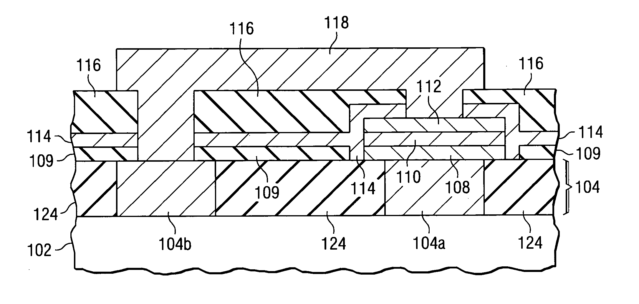
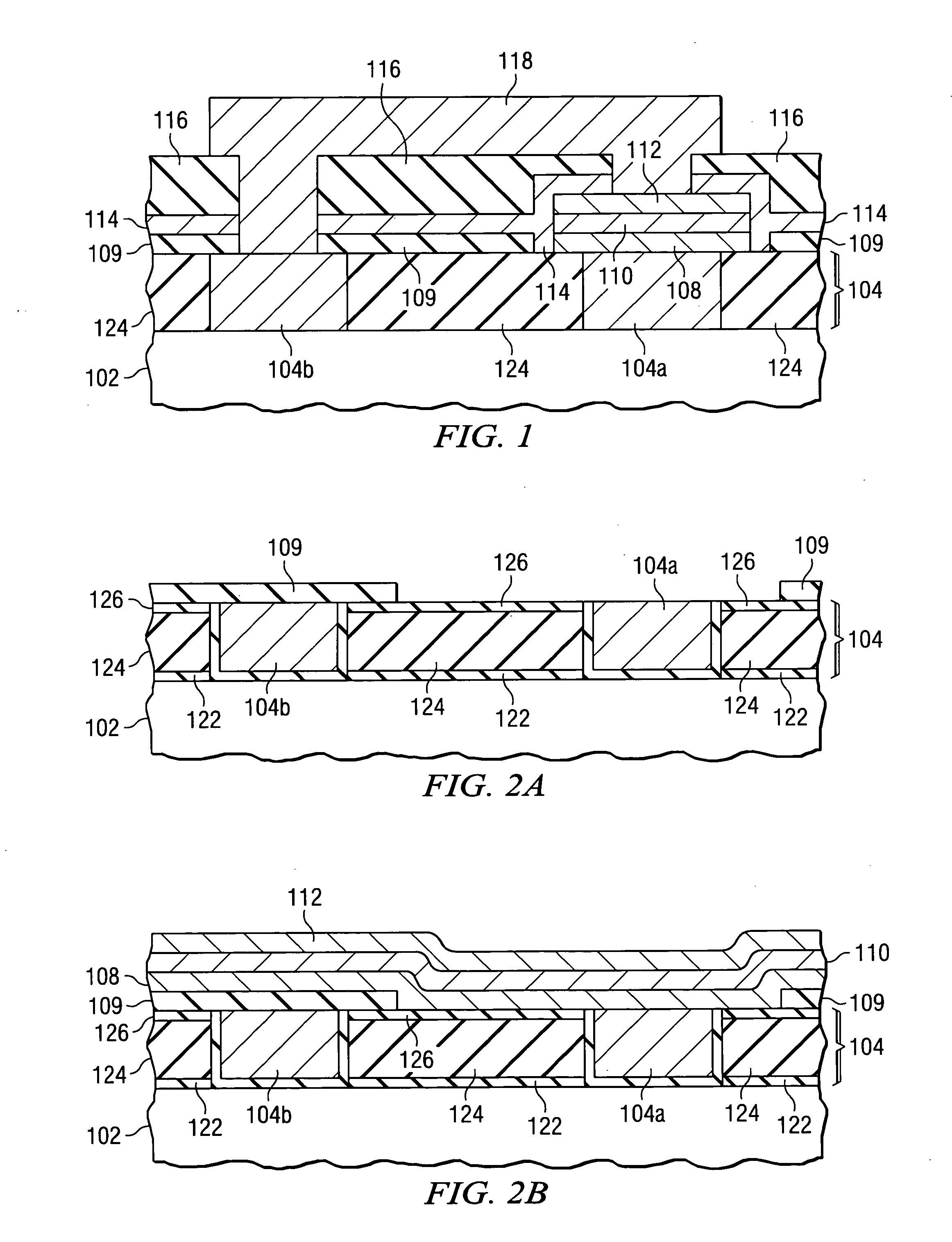
[0008] An advantage of the invention is providing on-chip de-coupling capacitance with surface protection for the metal / copper.

Problems solved by technology

This is due to the fact that smaller voltage swings can cause unacceptable amounts of current leakage and even unintentionally switch the state of the transistor.

Method used


Image

  • Capacitor integration at top-metal level with a protection layer for the copper surface
  • Capacitor integration at top-metal level with a protection layer for the copper surface
  • Capacitor integration at top-metal level with a protection layer for the copper surface

Examples


Embodiment Construction

[0013] The invention will now be described in conjunction with copper damascene process utilizing an aluminum cap layer. Those of ordinary skill in the art will appreciate that the benefits of the invention can be applied to other metal interconnect processes.

[0014] As semiconductor devices continue to scale, the decoupling capacitance requirements increase significantly. The parasitic resistance of off-chip capacitance can result in performance penalties. Placing the decoupling capacitors on-chip can reduce or even avoid these performance penalties. However, integrating the decoupling capacitors on-chip can cause other concerns. For example, using a gate oxide capacitor (in which a MOSFET gate oxide layer is also used as the capacitor dielectric) consumes active area. There are also leakage concerns with gate oxide capacitors. Adding a capacitor between contact and M1 (the first level of metal interconnect) adds a mask, may require routing restrictions above the capacitor and caus...


PUM

PropertyMeasurementUnit
supply voltageaaaaaaaaaa
operating voltagesaaaaaaaaaa
dielectric constantaaaaaaaaaa

Abstract

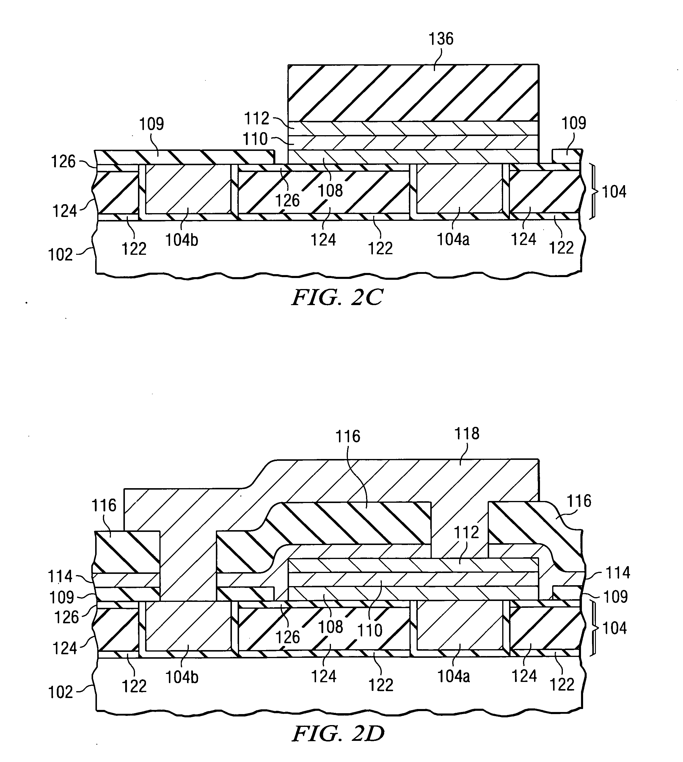
An on-chip decoupling capacitor (106) and method of fabrication. The decoupling capacitor (106) is integrated at the top metal interconnect level (104) and includes surface protection layer (109) for the copper metal (104b) of the top metal interconnect.

Description

CROSS-REFERENCE TO RELATED APPLICATIONS [0001] The following co-pending patent applications are related and hereby incorporated by reference: [0002] U.S. patent application No. (TI-35257), filed ______ to Rost et al. [0003] U.S. patent application No. (TI-35260), filed ______ to Burke et al.FIELD OF THE INVENTION [0004] The invention is generally related to the field of forming capacitors in semiconductor devices and more specifically to forming high density capacitors at the top metal interconnect level. BACKGROUND OF THE INVENTION [0005] As semiconductor technology continues to scale, the supply or operating voltage of the integrated circuit becomes lower and lower. The nominal supply voltage has decreased from 5V to 3.3V to 1.8V and below. Transistors with operating voltages of 1.1V are currently being developed. [0006] As the supply voltage decreases it becomes increasingly important to limit the voltage swing on the supply voltage lines. This is due to the fact that smaller vol...

Claims


Application Information

Patent Timeline
Patent Type & Authority Applications(United States)
IPC IPC(8): H01L21/02H01L23/522H10B12/00
CPCH01L23/5223H01L28/65H01L28/75H01L2924/0002H01L2924/00
Inventor PAPA RAO, SATYAVOLU S.ROST, TIMOTHY A.BURKE, EDMUND
Owner TEXAS INSTR INC
Learn More