

Circuit arrangement for reading out, evaluating and reading in again a charge state into a memory cell
a circuit arrangement and charge state technology, applied in static storage, digital storage, instruments, etc., can solve the problems of erroneous refresh, and the charge or voltage state cannot be written to the memory cell
- Summary
- Abstract
- Description
- Claims
- Application Information
AI Technical Summary
Benefits of technology
Problems solved by technology
Method used
Image

Examples
Embodiment Construction
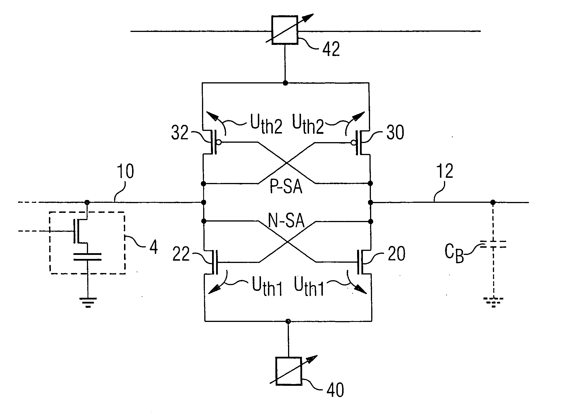
[0027]FIG. 1 shows a circuit arrangement with an identification of the threshold voltages UTH1 of the n-channel field-effect transistors and UTH2 of the p-channel field-effect transistors, which threshold voltages can be used according to the invention. A memory cell 4 with a storage capacitor and a selection transistor can be seen in the equivalent circuit diagram on the left, illustrated by broken lines. The memory cell 4 is coupled to a bit line 10 leading to the sense amplifier of the circuit arrangement. The sense amplifier comprises two cross-coupled CMOS inverters—or, considered from a different standpoint, one n-sense amplifier and one p-sense amplifier with in each case two field-effect transistors of the same conduction type. The bit line 10 is connected to the gate terminal of an n-channel field-effect transistor 20 and the gate terminal of a p-channel field-effect transistor 30. The two field-effect transistors 20, 30 are configured as CMOS inverters between two voltage ...
PUM
 Abstract
Description
Claims
Application Information