Inter-chip communication system

a communication system and chip technology, applied in the field of electronic design automation (eda), can solve the problems of burdening the user, requiring some degree of user sophistication, and cumbersome current software simulation and hardware emulation/acceleration, and achieve the effect of reducing performan

a communication system and chip technology, applied in the field of electronic design automation (eda), can solve the problems of burdening the user, requiring some degree of user sophistication, and cumbersome current software simulation and hardware emulation/acceleration, and achieve the effect of reducing performan

US20050102125A1Inactive Publication Date: 2005-05-12CADENCE DESIGN SYST INC

Image

  • Inter-chip communication system
  • Inter-chip communication system
  • Inter-chip communication system

Examples


Embodiment Construction

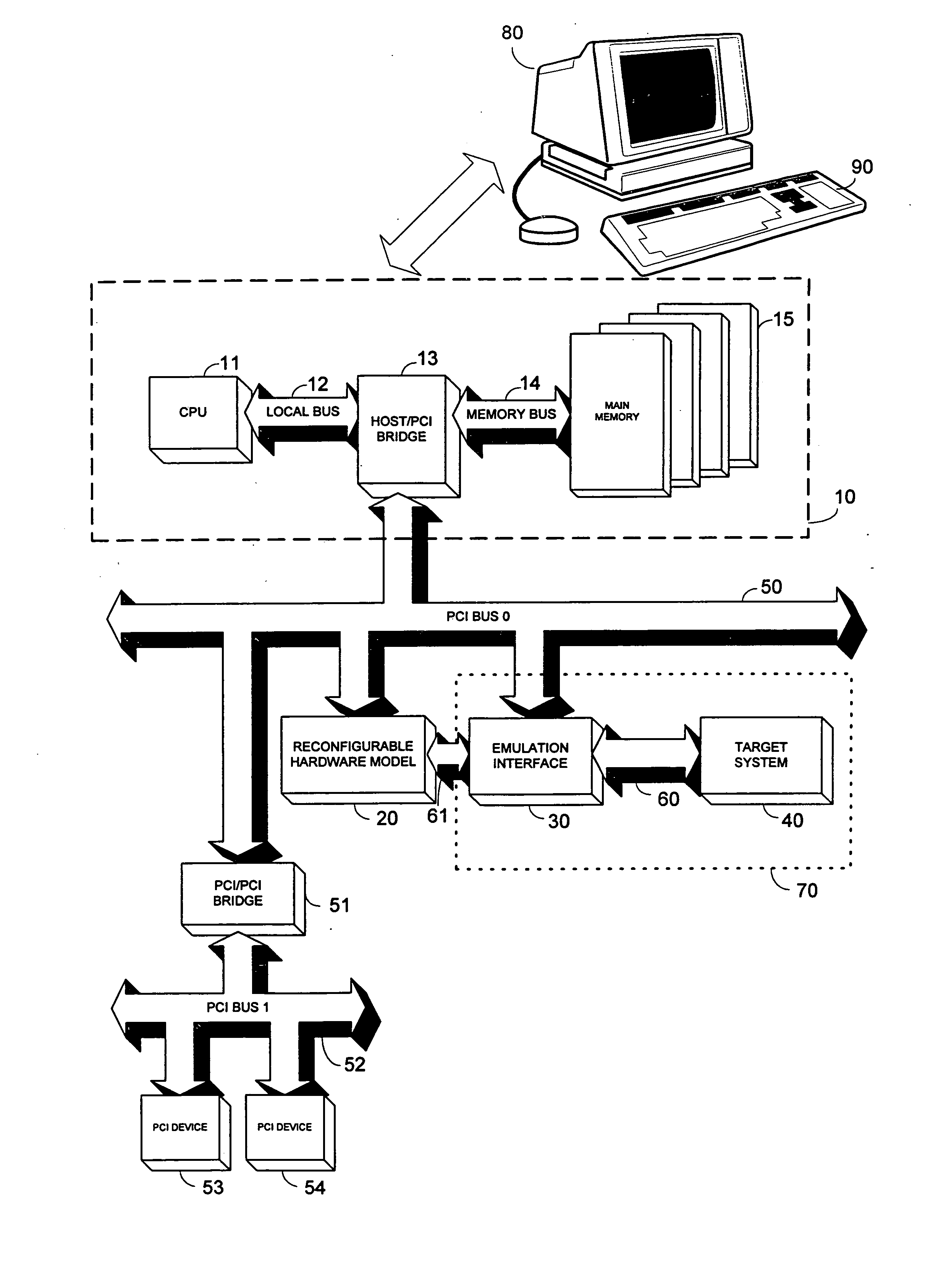
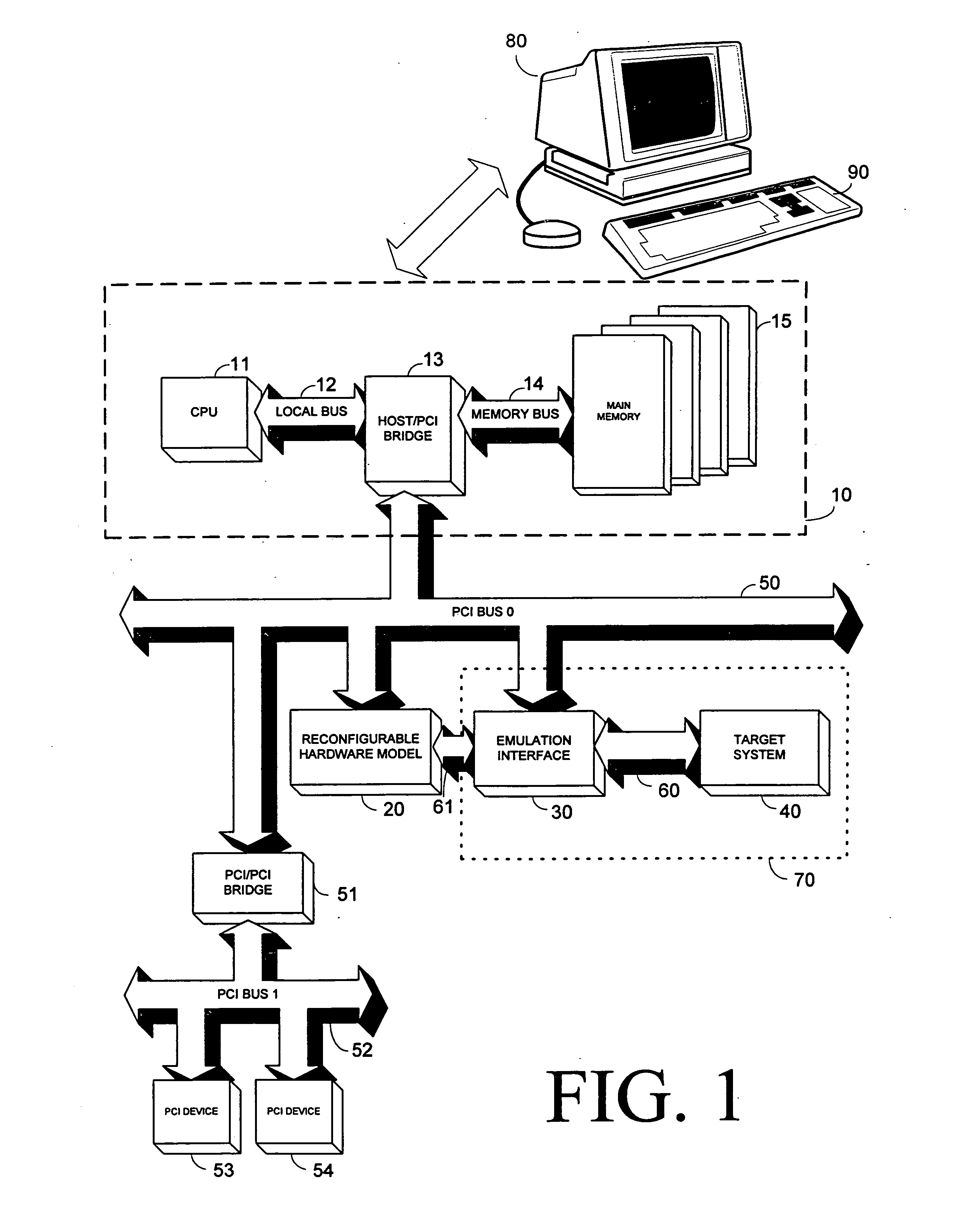
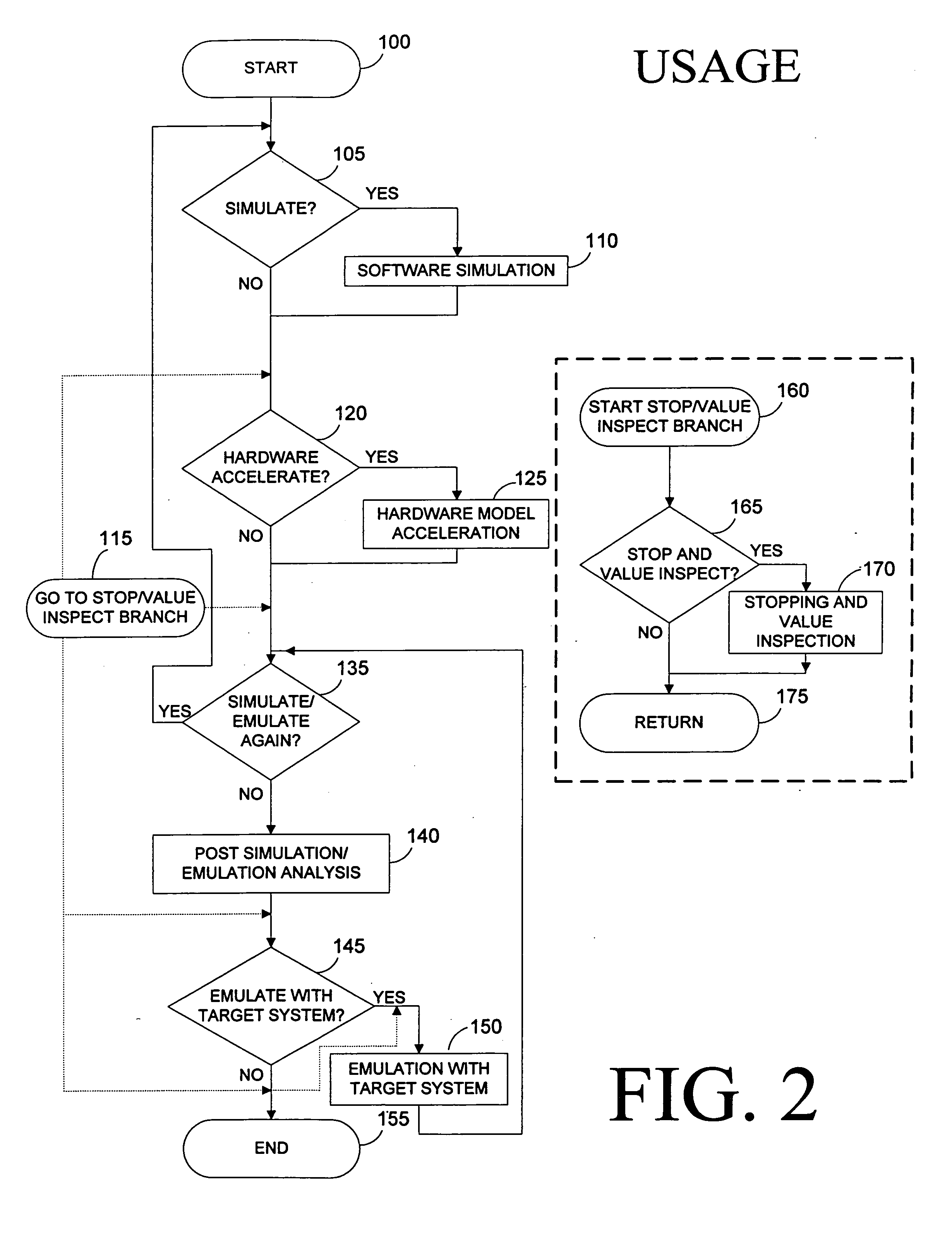
[0124] This specification will describe the various embodiments of the present invention through and within the context of a system called “SEmulator” or “SEmulation” system. Throughout the specification, the terms “SEmulation system,”“SEmulator system,”“SEmulator,” or simply “system” may be used. These terms refer to various apparatus and method embodiments in accordance with the present invention for any combination of four operating modes: (1) software simulation, (2) simulation through hardware acceleration, (3) in-circuit emulation (ICE), and (4) post-simulation analysis, including their respective set-up or pre-processing stages. At other times, the term “SEmulation” may be used. This term refers to the novel processes described herein.

[0125] Similarly, terms such as “Reconfigurable Computing (RCC) Array System” or “RCC computing system” refers to that portion of the simulation / coverification system that contains the main processor, software kernel and the software model of t...


PUM


Abstract

The complexity of user designs, the limited capacity of FPGA chips, and the limited number of chip pinouts have resulted in the development of inter-chip communication technology that necessitates the transfer of a large amount of data across a limited number of pins in the shortest amount of time. The inter-chip communication system transfers signals across FPGA chip boundaries only when these signals change values. Thus, no cycles are wasted and every event signal has a fair chance of achieving communication across chip boundaries. The inter-chip communication system includes a series of event detectors that detect changes in signal values and packet schedulers which can then schedule the transfer of these changed signal values to another designated chip. Working with a plurality of signal groups that represents signals at the separated connections, the event detector detects events (or changes in signal values). When an event has been detected, the event detector alerts the packet scheduler. The packet scheduler employs a token ring scheme as follows. When the packet scheduler receives a token and detects an event, the packet scheduler “grabs” the token and schedules the transmission of this packet in the next packet cycle. If, however, the packet scheduler receives the token but does not detect an event, it will pass the token to the next packet scheduler. At the end of each packet cycle, the packet scheduler that grabbed the token will pass the token to the next logic associated with another packet.

Description

RELATED U.S. APPLICATION [0001] This is a continuation-in-part of U.S. patent application Ser. No. 09 / 373,014, filed with the United States Patent and Trademark Office on Aug. 11, 1999, which is a continuation-in-part application of U.S. patent application Ser. No. 09 / 144,222, filed Aug. 31, 1998.BACKGROUND OF THE INVENTION [0002] 1. Field of the Invention [0003] The present invention generally relates to electronic design automation (EDA). More particularly, the present invention relates to dynamically changing the evaluation period to accelerate design debug sessions. [0004] 2. Description of Related Art [0005] In general, electronic design automation (EDA) is a computer-based tool configured in various workstations to provide designers with automated or semi-automated tools for designing and verifying user's custom circuit designs. EDA is generally used for creating, analyzing, and editing any electronic design for the purpose of simulation, emulation, prototyping, execution, or ...

Claims


Application Information

Patent Timeline
12 May 2005
Publication
US20050102125A1
IPC
G06F13/22; G06F13/42; G06F17/50
CPC
G06F13/22; G06F17/5027; G06F17/5022; G06F13/4291; G06F30/331; G06F30/33
Inventors
TSENG, PING-SHENG