Layer transfer of low defect SiGe using an etch-back process

a layer transfer and etching technology, applied in the direction of crystal growth process, chemistry apparatus and processes, transistors, etc., can solve the problems of limiting the full implementation of high-speed devices, increasing the cost of high-speed devices, and several limits of methods, so as to and reduce the cost of high-speed devices.

Inactive Publication Date: 2005-05-19
GLOBALFOUNDRIES INC
View PDF23 Cites 21 Cited by
  • Summary
  • Abstract
  • Description
  • Claims
  • Application Information

AI Technical Summary

Benefits of technology

[0008] The invention provides a method capable of transferring a low defect SiGe layer onto a desirable substrate using the etch-back method but without any additional heavily doped etch-stop layer. The key feature of this invention is that a SiGe layer serves both as the layer over which the epitaxial strained Si / SiGe is grown but also as an etch-stop layer itself in some specific etching solutions. In other words, the SiGe layer is a self-etch-stop in this case. As a result, the process of fabricating strained Si / SiGe on insulator or a SiGe / Si heterostucture is greatly simplified and the quality of the strained Si / SiGe or SiGe / Si heterostucture is significantly improved.

Problems solved by technology

However, the underlying conducting substrate for MODFETs and HBTs or the interaction of the underlying substrate with active device region in CMOS are undesirable features which limit the full implementation of high speed devices.
However, this method has several limits because the oxygen implantation induces further damages in the relaxed SiGe layer in addition to the existing defects caused by lattice mismatch.
And, the high temperature anneal (>1100° C.) needed to form oxide after the oxygen implantation is detrimental to the strained Si / SiGe layers since Ge tends to diffuse and agglomerate at temperatures above 600° C., this effect becomes more significant when Ge content is higher than 10%.
However, the alloy then no longer behaves like the bulk material due to the quantum size effect.

Method used


Image

  • Layer transfer of low defect SiGe using an etch-back process
  • Layer transfer of low defect SiGe using an etch-back process
  • Layer transfer of low defect SiGe using an etch-back process

Examples


Embodiment Construction

[0016] The embodiment which will now be described in conjunction with the above drawings relates to the formation of a layer of monocrystalline strained Si / SiGe on an insulator material (SGOI) or a SiGe layer on Si with the aid of planarization of surfaces, wafer bonding and a selective wet etching process using SiGe as the etch-stop layer.

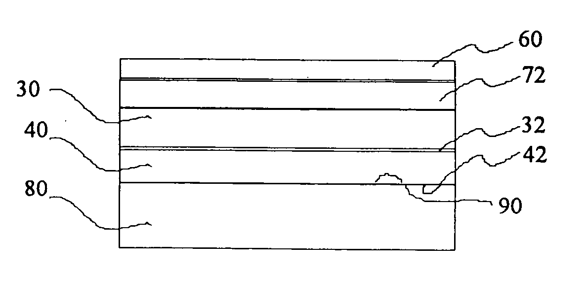
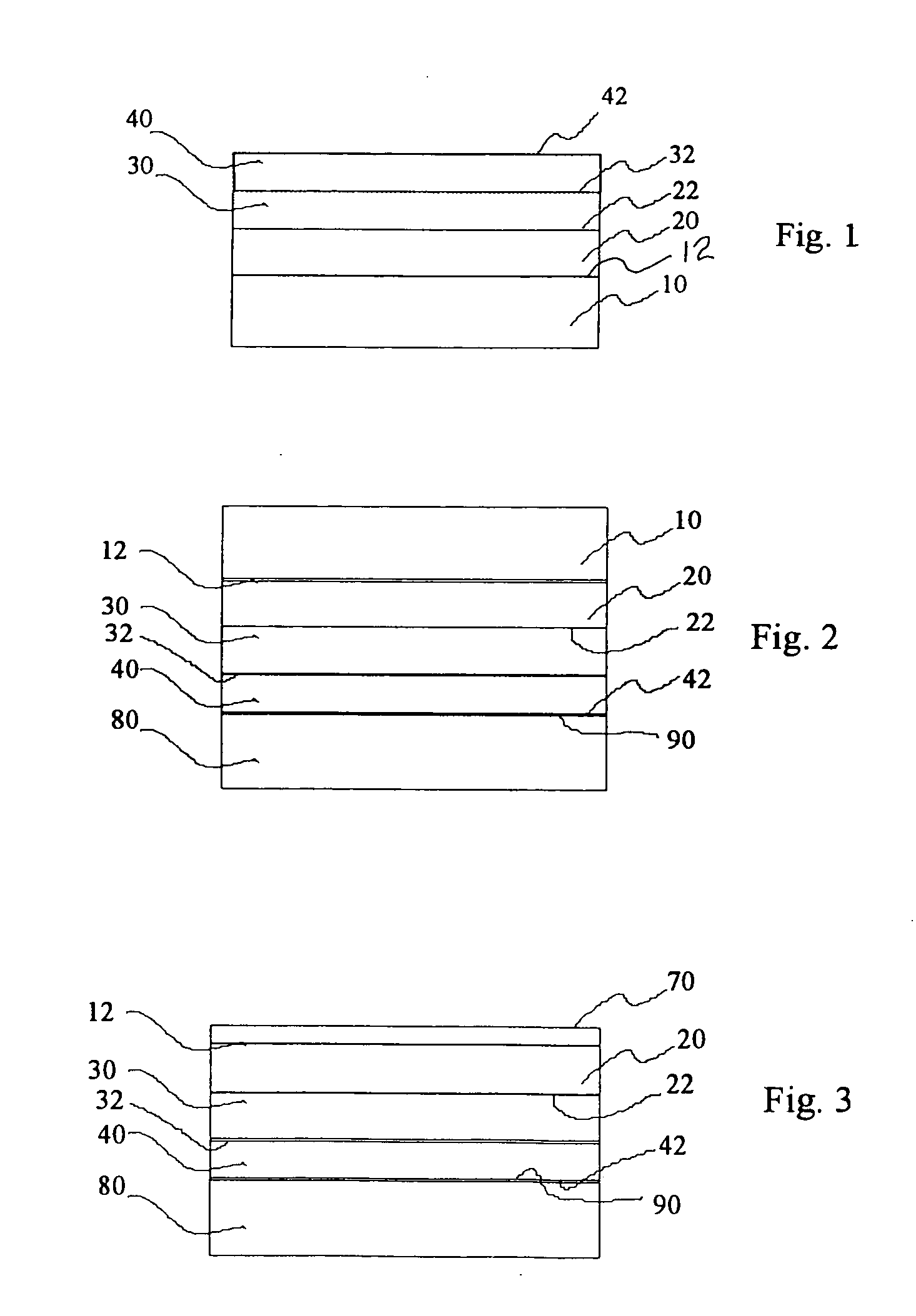
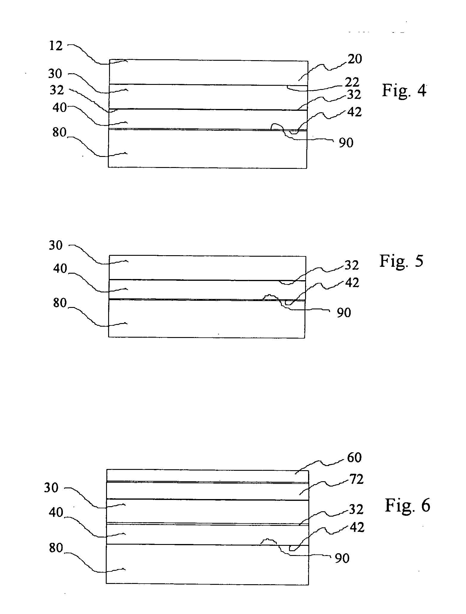
[0017] Referring now to FIG. 1, a cross section view of a partial embodiment of the invention is shown comprising a substrate 10 and a plurality of layers 20, 30 and 40. Substrate 10 may be a single crystal material such as Si, SiGe, SiGeC, SiC etc. suitable for forming epitaxial layers thereon. An epitaxial graded layer 20 of Si1−xGex is formed on the upper surface 12 of substrate 10. The upper surface 22 of graded layer 20 is substantially relaxed or completely relaxed. The relaxation may be due to a modified Frank-Read mechanism described by LeGoues et al. in U.S. Pat. No. 5,659,187 which issued on Aug. 19, 1997 and is incorporated herein by r...


PUM

PropertyMeasurementUnit
surface roughnessaaaaaaaaaa
thicknessaaaaaaaaaa
temperatureaaaaaaaaaa

Abstract

A method for forming strained Si or SiGe on relaxed SiGe on insulator (SGOI) or a SiGe on Si heterostructure is described incorporating growing epitaxial Si1−yGey layers on a semiconductor substrate, smoothing surfaces by Chemo-Mechanical Polishing, bonding two substrates together via thermal treatments and transferring the SiGe layer from one substrate to the other via highly selective etching using SiGe itself as the etch-stop. The transferred SiGe layer may have its upper surface smoothed by CMP for epitaxial deposition of relaxed Si1−yGey, and strained Si1−yGey depending upon composition, strained Si, strained SiC, strained Ge, strained GeC, and strained Si1−yGeyC or a heavily doped layer to make electrical contacts for the SiGe / Si heterojunction diodes.

Description

FIELD OF INVENTION [0001] This invention relates to transferring a SiGe layer onto a second substrate and forming a new material structure that has emerging applications in microelectronics and optoelectronics. In particular, a strained Si / SiGe layer on an insulator structure is useful for fabricating high speed devices such as complementary metal oxide semiconductor (CMOS) transistors, modulation doped field effect transistors (MODFETs), high electron mobility transistors (HEMTs), and bipolar transistors (BTs); SiGe layer on Si heterostructures can be used to produce photodetectors to provide Si-based far infrared detection for communication, surveillance and medical applications. BACKGROUND OF THE INVENTION [0002] For applications in microelectronics, high carrier mobilities are desirable. It has been found that electron mobility in strained Si / SiGe channels is significantly higher than that in bulk Si. For example, measured values of electron mobility in strained Si at room tempe...

Claims


Application Information

Patent Timeline
Patent Type & Authority Applications(United States)
IPC IPC(8): H01L21/02H01L21/20H01L21/336H01L21/338H01L21/331H01L21/762H01L27/12H01L29/161H01L29/737H01L29/778H01L29/786H01L29/812H01L29/861H01L31/10
CPCH01L21/76256H01L21/2007H01L21/20
Inventor CHU, JACK OONDIMILIA, DAVID R.HUANG, LIJUAN
Owner GLOBALFOUNDRIES INC
Why Eureka
Try Eureka