Wafer-level package and its manufacturing method

a manufacturing method and package technology, applied in the field of wafer-level packages, can solve the problems of complex process for forming the via hole, the trade-off between the formation of the via hole and the embedding of the via metal becomes the problem, and the band characteristics of parametric inductance degrades

Inactive Publication Date: 2005-05-19
KK TOSHIBA
View PDF4 Cites 85 Cited by
  • Summary
  • Abstract
  • Description
  • Claims
  • Application Information

AI Technical Summary

Problems solved by technology

One of the major problems of the wafer-level package is how to connect internal bonding pads on a substrate surface to external electrode pads on an outer surface of the package.
However, by the above-mentioned first and third methods, when a frequency becomes over gigahertz-band, the problem that parasitic inductance degrades a band characteristics arise in a high frequency circuit.
By the second method, the trade-off between the formation of the via hole and embedment of the via metal becomes the problem.
On the other hand, if the via hole has several micrometers diameter and large aspect ratio, complicated process for forming the via hole is needed, such as repeating etching and forming protective layer of sidewalls of the via hole.
Further, in the case of embedding a conductive layer (a part of which may be an insulator) in the via hole, if the via hole has a large diameter of tens of micrometers, a long processing time is needed, such as embedding the precise conductive layer of tens of micrometers thickness by a process for thin film including in thin film the conductive layer sputtering, CVD, and plating.
Additionally, if the via hole has large diameter, a problem also occurs that an integration density of the via hole falls.
Thus, the method of connecting internal bonding pads to external bonding pads has a problem that the via hole of small diameter is hard to be etched and the via hole of large diameter is hard to be embedded in.

Method used


Image

  • Wafer-level package and its manufacturing method
  • Wafer-level package and its manufacturing method
  • Wafer-level package and its manufacturing method

Examples


first embodiment

[0082]FIG. 3 through FIG. 10 show process steps for manufacturing the wafer-level package according to the first example of the invention.

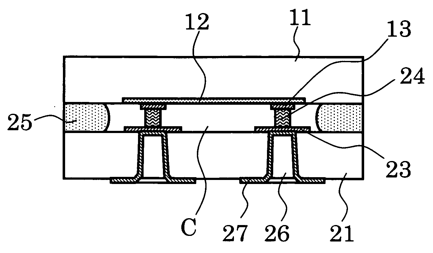
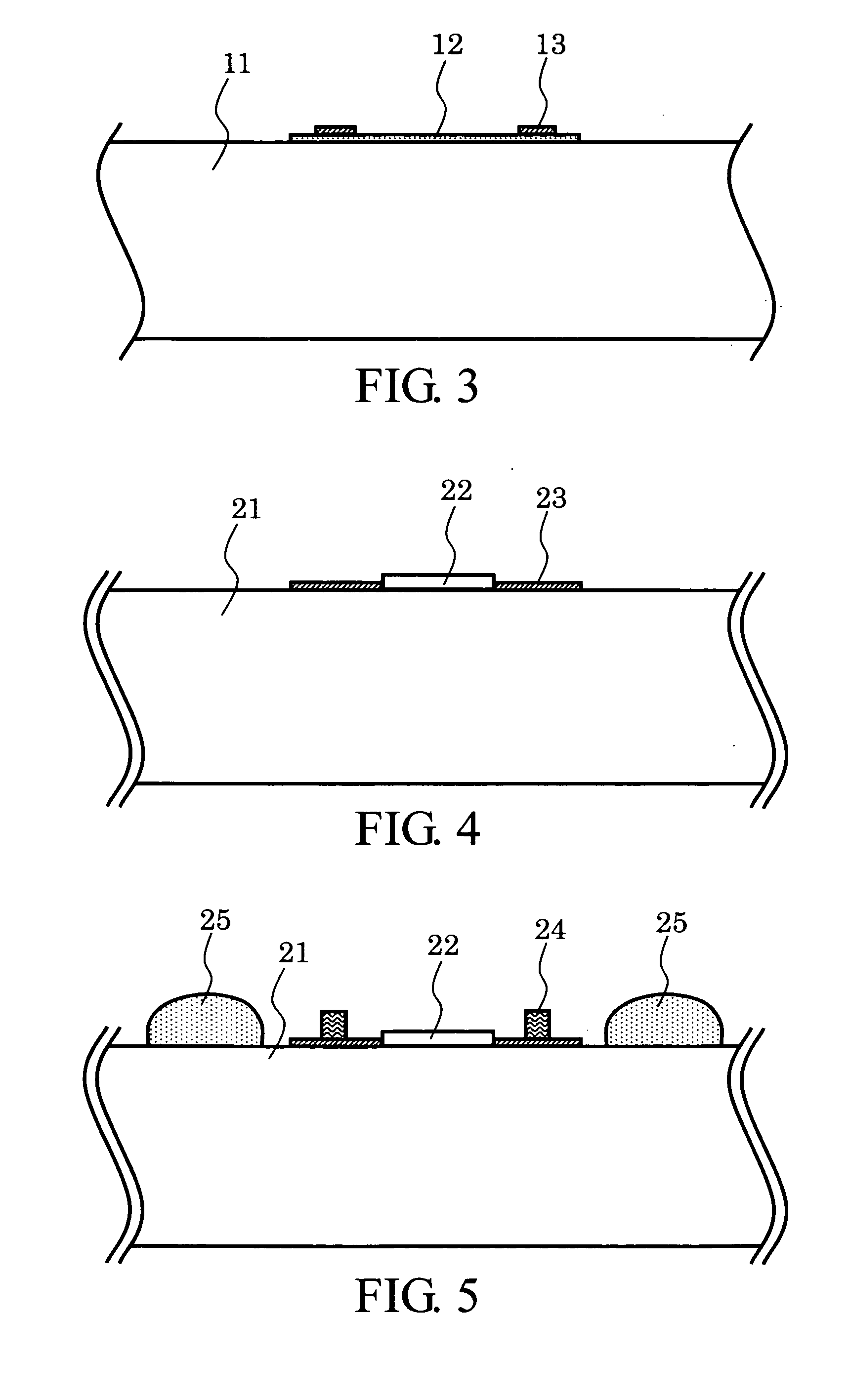
[0083] In FIG. 3, the first internal electrode pads 13 of Aluminum (Al) etc. and the semiconductor device 12 are provided on the surface of the first substrate 11 of silicon (Si) by a well-known method. The first substrate 11 may be an entire wafer or a divided wafer. It is desirable that the first substrate 11 has enough area to dispose a plurality of semiconductor chips thereon.

[0084] In FIG. 4, a FBAR 22 and the second internal electrode pads 23 of Aluminum (Al) etc. are provided on the surface of the second substrate 21 of silicon (Si) prepared separately by a well-known method. The second substrate 21 may be an entire wafer or a divided wafer. The second substrate 21 is needed to have the same shape as the first substrate 11 substantially.

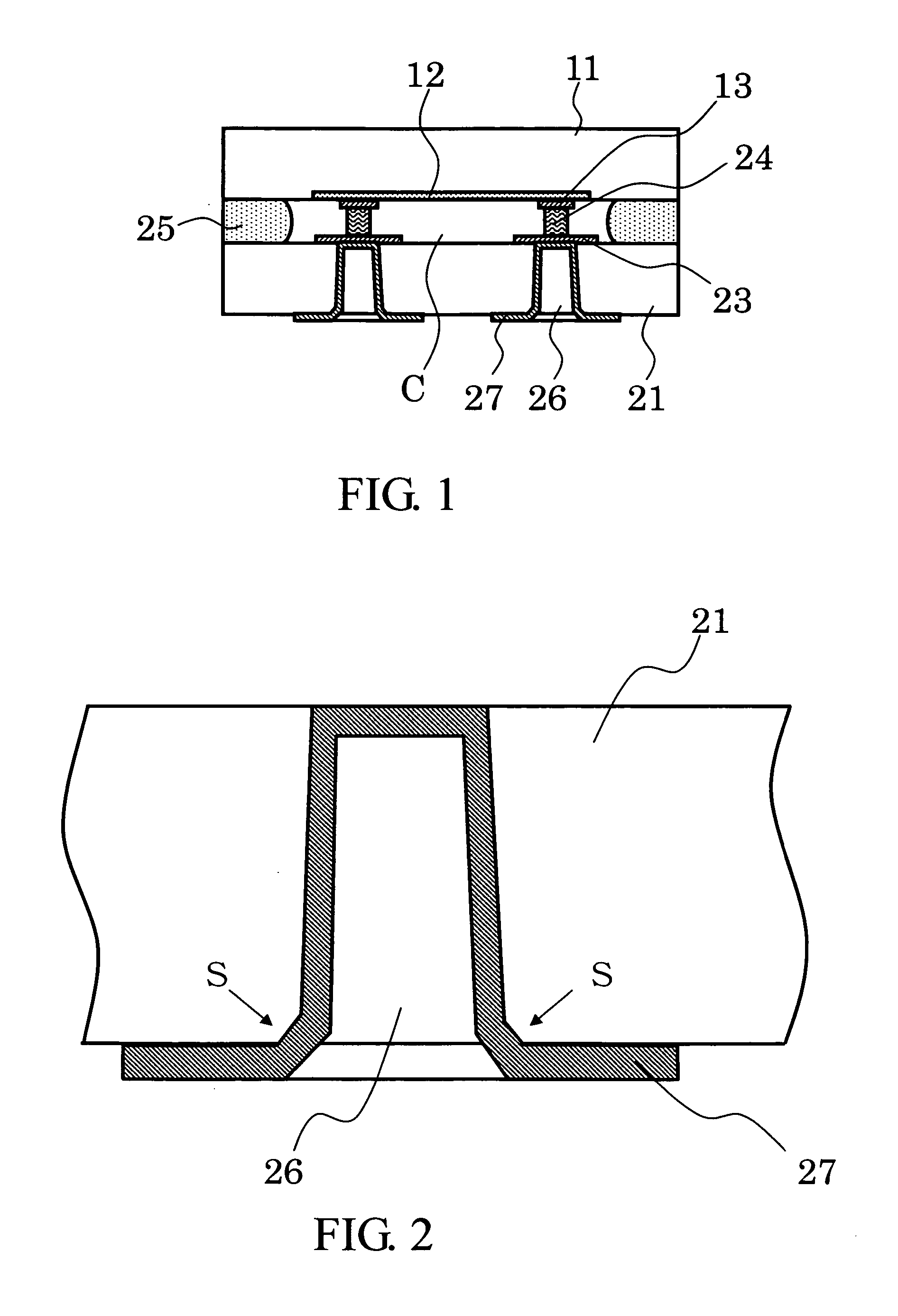
[0085] In FIG. 5, stud bumps 24 are formed on the second internal electrode pads 23 using bonding wire...

second embodiment

[0093] Since the process steps of the second example before the process steps mentioned above in FIG. 9 are the same as that of the first example, only the subsequent process steps will be explained.

[0094]FIG. 11 through FIG. 13 show process steps for manufacturing the wafer-level package according to the second example of the invention. In FIG. 11, after the process step shown in FIG. 9, the trenches 28 are formed by half-cutting the regions stuck with sealing resin 25 using a dicing saw of 200 micrometers width to the second substrate 21 from the back side of the first substrate 11.

[0095] In FIG. 12, the backside of the first substrate 11 is covered with the adhesive resin 29 and is cured.

[0096] In FIG. 13, dicing is performed using the dicing saw of 30 micrometers width, and the central parts of the trenches 28 are separated for every chip.

[0097] By such processes, in addition to the same effect as the first example, since the sides of the package are doubly covered with the ...

third embodiment

[0098]FIG. 14 through FIG. 21 are process steps for manufacturing method of the wafer-level package according to the third example of the invention.

[0099] In FIG. 14, a microswitch 22 and the second internal electrode pads 23 of aluminum are provided on the surface of the second substrate 21 of Si by a well-known method. The second substrate 21 may be an entire wafer or a divided wafer. It is desirable that the second substrate 21 is the same shape as the first substrate 11. Further, the adhesive resin 25 are printed by screen-print along the periphery of the microswitch 22 and the second internal electrode pads 23.

[0100] Moreover, in FIG. 15, the semiconductor device 12 and the first internal electrode pads 13 of aluminum are provided on the surface of the first substrate 11 of Si by a well-known method.

[0101] In FIG. 16, conductive resin 14 is printed on the first internal electrode pads 13 using screen printing.

[0102] Next, as shown in FIG. 17, the first substrate 11 and the ...


PUM


Abstract

A wafer-level package comprises: a first substrate; an electric element provided on the first substrate; a second substrate; an internal electrode pad; a well; and an external electrode pad. The second substrate is opposed to the first substrate with a predetermined gap therebetween. The electric element is provided between the first and second substrates. The internal electrode pad extends onto a first surface of one of the first and the second substrates. The inner electrode pad is connected to the electric element. The well penetrates the one of the first and the second substrates to the internal electrode. The external electrode pad is provided on a second surface of the one of the first and the second substrates and extends onto an inner wall of the well and being connected with the internal electrode pad.

Description

CROSS-REFERENCE TO RELATED APPLICATIONS [0001] This application is based upon and claims the benefit of priority from the prior Japanese Patent Application No. 2003-341982, filed on Sep. 30, 2003; the entire contents of which are incorporated herein by reference. BACKGROUND OF THE INVENTION [0002] The present invention relates to a wafer-level package and its manufacturing method. More specifically, the invention relates to a wafer-level package which has a cavity inside the package and is suitable for a high frequency circuit or an analog circuit having small number of connecting pins, and its manufacturing method. [0003] Recently, a package has been highly desired to be small sized, thin and inexpensive. Particularly, in high frequency circuit, such a package has been needed for a small-sized mobile equipment in accordance with upgrading and diversifying of the wireless communication systems. For this reason, a wafer-level package is paid an attention, as an ultimate package, in w...

Claims


Application Information

Patent Timeline
Patent Type & Authority Applications(United States)
IPC IPC(8): H01L21/48H01L21/60H01L23/12H01L23/055H01L23/14H01L23/498H01L25/065H01L25/07H01L25/18H03H3/02H03H9/02H03H9/10H03H9/17
CPCB81B2207/096H01L2224/16235H01L21/486H01L23/055H01L23/147H01L23/49827H01L24/81H01L24/83H01L24/94H01L2224/16H01L2224/81801H01L2224/83191H01L2224/838H01L2924/01005H01L2924/01013H01L2924/01078H01L2924/01079H01L2924/01082H01L2924/0781H01L2924/15313H01L2924/163H01L2924/19041H01L2924/19042H01L2924/30107H03H9/0547H03H9/105H01L24/29H01L2924/01006H01L2924/01033H01L2224/14051H01L2224/81191H01L2224/81193B81C1/00301H01L2224/05573H01L2224/05568H01L2224/05624H01L24/05H01L2924/00014
Inventor KAWAKUBO, TAKASHIYASUMOTO, TAKAAKIITAYA, KAZUHIKO
Owner KK TOSHIBA
Why Eureka
Try Eureka