
Method of verifying circuitry used for testing a new logic component prior to the first release of the component

a technology of logic components and verification environments, applied in the direction of functional testing, error detection/correction, instruments, etc., can solve the problems of inability to fully test or verify the component or product, difficult or substantially impossible to have confidence that the logic or verification environment is functioning properly, and the component or product cannot be fully tested or verified. , to achieve the debugging of the component or dut, the debugging can only be accomplished by a properly operating verification environmen

Inactive Publication Date: 2005-05-19
TEXAS INSTR INC
View PDF5 Cites 16 Cited by
  • Summary
  • Abstract
  • Description
  • Claims
  • Application Information

AI Technical Summary

Problems solved by technology

Unfortunately, it is difficult or substantially impossible to have confidence that the logic or verification environment is functioning properly without having a component or product known to be operating properly that can be tested, evaluated, and “passed” by the environment verification circuitry.
On the other hand, it is impossible to fully test or verify the component or product unless the logic environment is known to be functioning properly.
Yet, acceptable debugging of the component or DUT can only be accomplished by a properly operating verification environment.
However, now with millions and millions of circuits to be tested on a single device, such a “start-stop and then correct the problem approach regardless of whether the problem was in the environmental or in the device” has become exponentially more complex and is simply unacceptable and too costly.
This traditional solution is both complex, time consuming, and of course expensive.
This risky approach may end up being more costly and time consuming than the traditional approach discussed above.

Method used

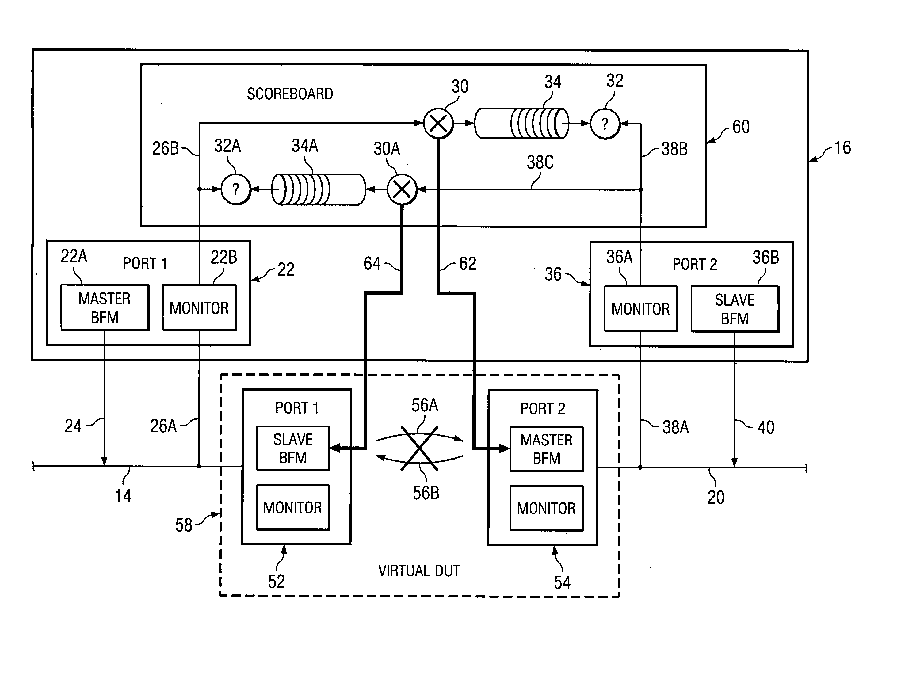
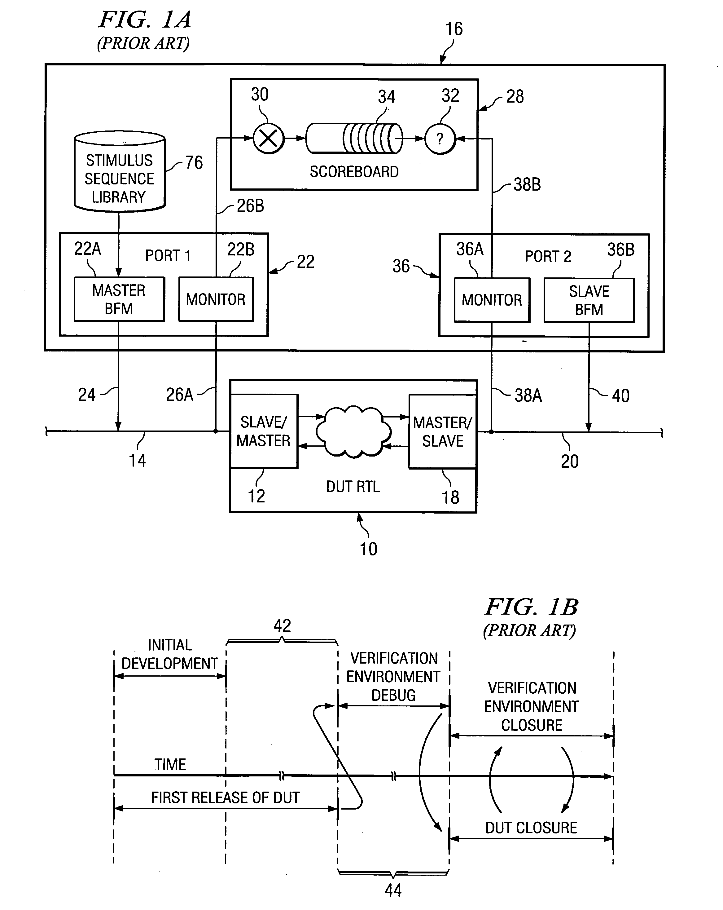
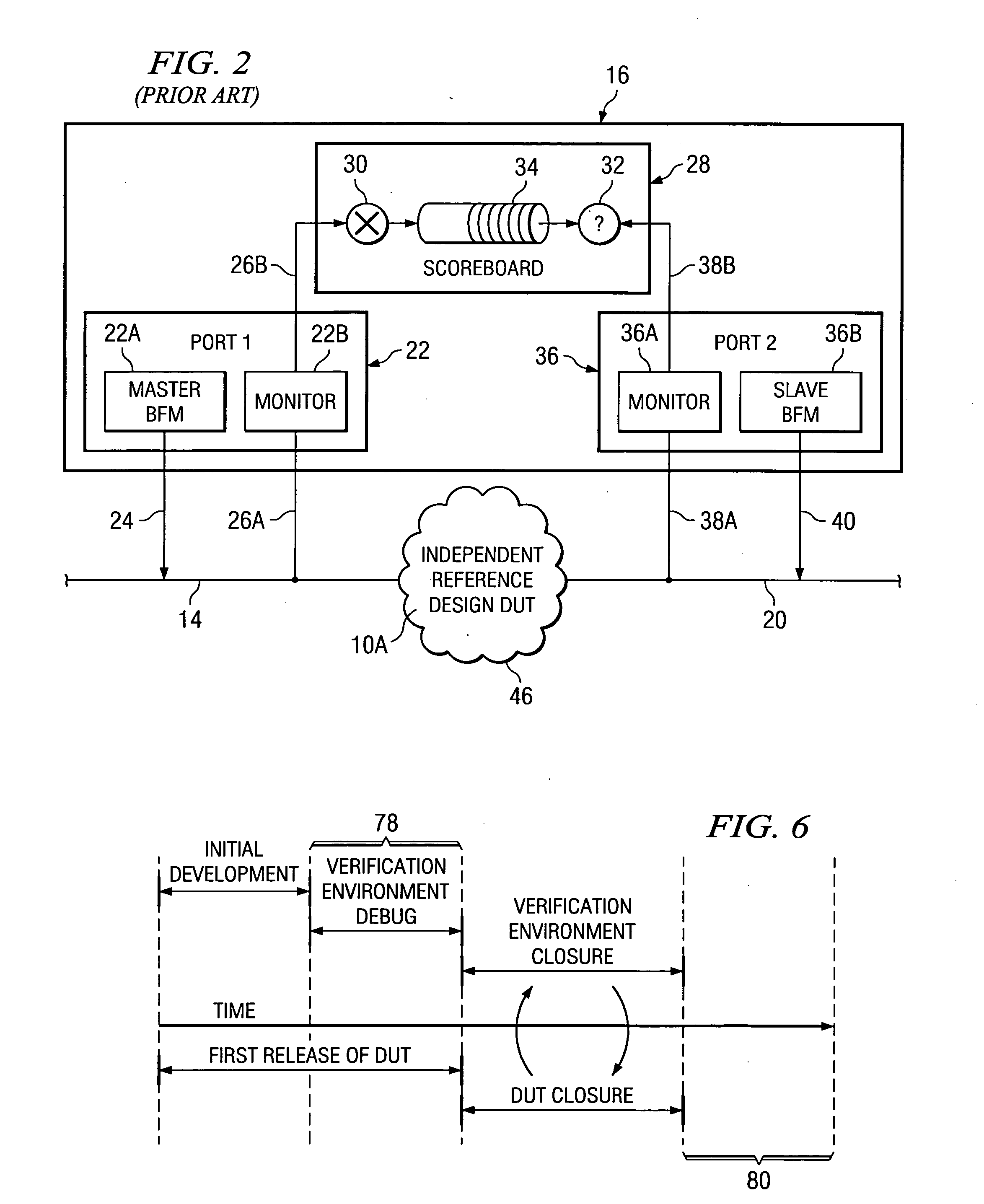

Image

  • Method of verifying circuitry used for testing a new logic component prior to the first release of the component
  • Method of verifying circuitry used for testing a new logic component prior to the first release of the component
  • Method of verifying circuitry used for testing a new logic component prior to the first release of the component

Examples


Embodiment Construction

[0019] Apparatus and method embodiments are discussed in detail below. It should be appreciated, however, that the present invention provides many applicable inventive concepts that can be embodied in a wide variety of specific contexts. The specific embodiments discussed are merely illustrative of specific ways to make and use the invention, and do not limit the scope of the invention.

[0020] As was discussed above, because of the ever increasing complexity of IC designs, it has become necessary to develop effective and efficient automated verification environments. A known stable and dependable verification environment is critical in verifying the component or DUT (Device Under Test) if the verification or testing results carried out on the DUT is to have any credibility. Unfortunately, however, with complex components or devices and presently available technology, the verification environment cannot be considered fully stable and dependable for testing a device until it has been ...


PUM


Abstract

A method and operation for developing and testing the logic environment used for providing logic inputs to and receiving logic inputs from a logic device or device under test such as an ASIC device prior to the completion of the device production design. The invention eliminates much of the waiting time typically required for determining whether problems are due to design errors in the DUT or incorrect operation of the environment used to test and develop the DUT.

Description

[0001] This application claims the benefit of U.S. Provisional Application No. 60 / 505,853, filed on Sep. 25, 2003, entitled A METHODOLOGY FOR ACCELERATING NEW PRODUCT DEVELOPMENT, which application is hereby incorporated herein by reference.TECHNICAL FIELD [0002] The present invention relates to the development and testing of new complex semiconductor products such as ASIC's (Application Specific Integrated Circuit) or other logic components, and more specifically for testing the “correctness” of the logic or verification environment before the product or device (DUT) is released and available for testing. BACKGROUND [0003] Presently available basic products and other complex semiconductor devices often include several millions or more individual logic circuits that must be tested or proven before released for sale and / or distribution. However, in addition to checking the operation of the product or component, it is also necessary to test or verify the correctness of the component o...

Claims


Application Information

Patent Timeline
Patent Type & Authority Applications(United States)
IPC IPC(8): G06F11/00G06F11/26G06F11/267
CPCG06F11/261G06F11/2215
Inventor DEATON, CRAIG F.
Owner TEXAS INSTR INC
Learn More