

Multilayer metallization
a multi-layer, metallization technology, applied in the direction of semiconductor devices, semiconductor/solid-state device details, electrical apparatus, etc., can solve the problems of failure, failure, and difficulty in solving the step coverage problem of conventional cvd techniques, let alone pvd techniques,
- Summary
- Abstract
- Description
- Claims
- Application Information
AI Technical Summary
Problems solved by technology
Method used
Image

Examples
Embodiment Construction
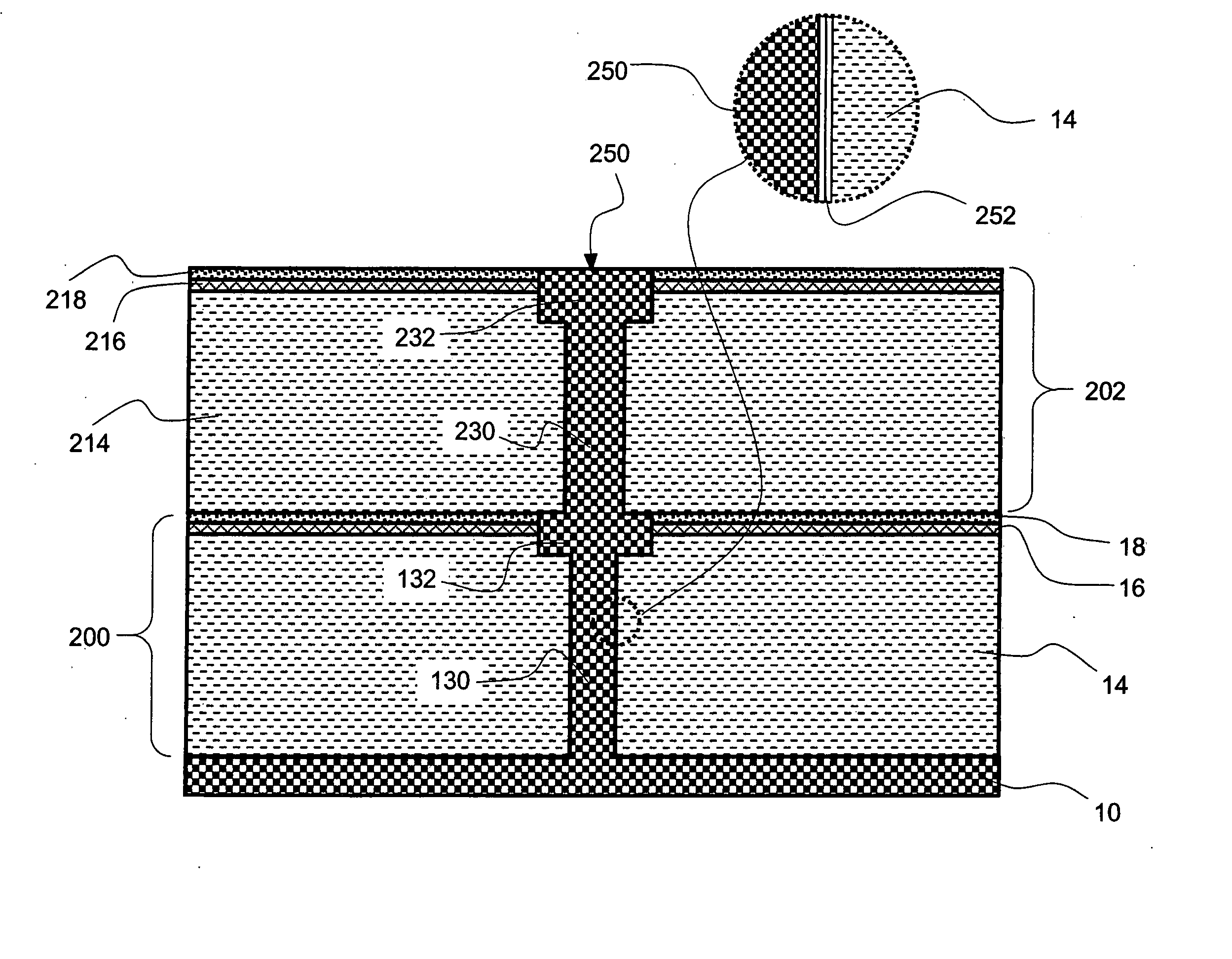
[0033] Preferred embodiments of the invention address many of the problems discussed above by providing structures and methods in which one or more conductive elements can be formed after the formation of one or more overlying layers of material. As such, the conductive element and the space into which the conductive element is deposited are both buried features, i.e., both features are buried in the sense that an overlying material covers at least part of these features. Rather than depositing mutually contacting conductors in multiple stages, e.g., forming metallization layers and filling vias and trenches in different stages as different levels of these structures are formed, in the preferred embodiments the space for accommodating these conductors are preferably held open or temporarily filled with a sacrificial material. These spaces are then all opened. Subsequently, the openings are simultaneously filled with bulk conductor, before deposition of further overlying layers. Adva...
PUM
 Abstract
Description
Claims
Application Information