Double-faced detecting devices for an electronic substrate

a detection device and electronic substrate technology, applied in the direction of measurement devices, printed circuit testing, instruments, etc., can solve the problems of only simulating data that is not precise, 80% of electronic substrates can be modified and detected by the conventional detection device, and the rest of the electronic substrates cannot be modified

Inactive Publication Date: 2005-06-02
PREMTEK INT
View PDF3 Cites 30 Cited by
  • Summary
  • Abstract
  • Description
  • Claims
  • Application Information

AI Technical Summary

Benefits of technology

[0005] The present invention provides double-faced detecting devices for an electronic substrate in high-frequency properties, which conveniently contact multiple detecting points on two faces of the electronic substrate to detect the high-frequency properties.

Problems solved by technology

Unfortunately, data of high-frequency properties obtained from the designed wafers or the printed circuit boards are only simulating data that is not precise.
Additionally, only 80% of the electronic substrates can be modified and be detected by the conventional detecting devices.
Rest of the electronic substrate still can not be modified in circuit to arrange the multiple detecting points on the same face and thus can not be detected.

Method used


Image

  • Double-faced detecting devices for an electronic substrate
  • Double-faced detecting devices for an electronic substrate
  • Double-faced detecting devices for an electronic substrate

Examples


Embodiment Construction

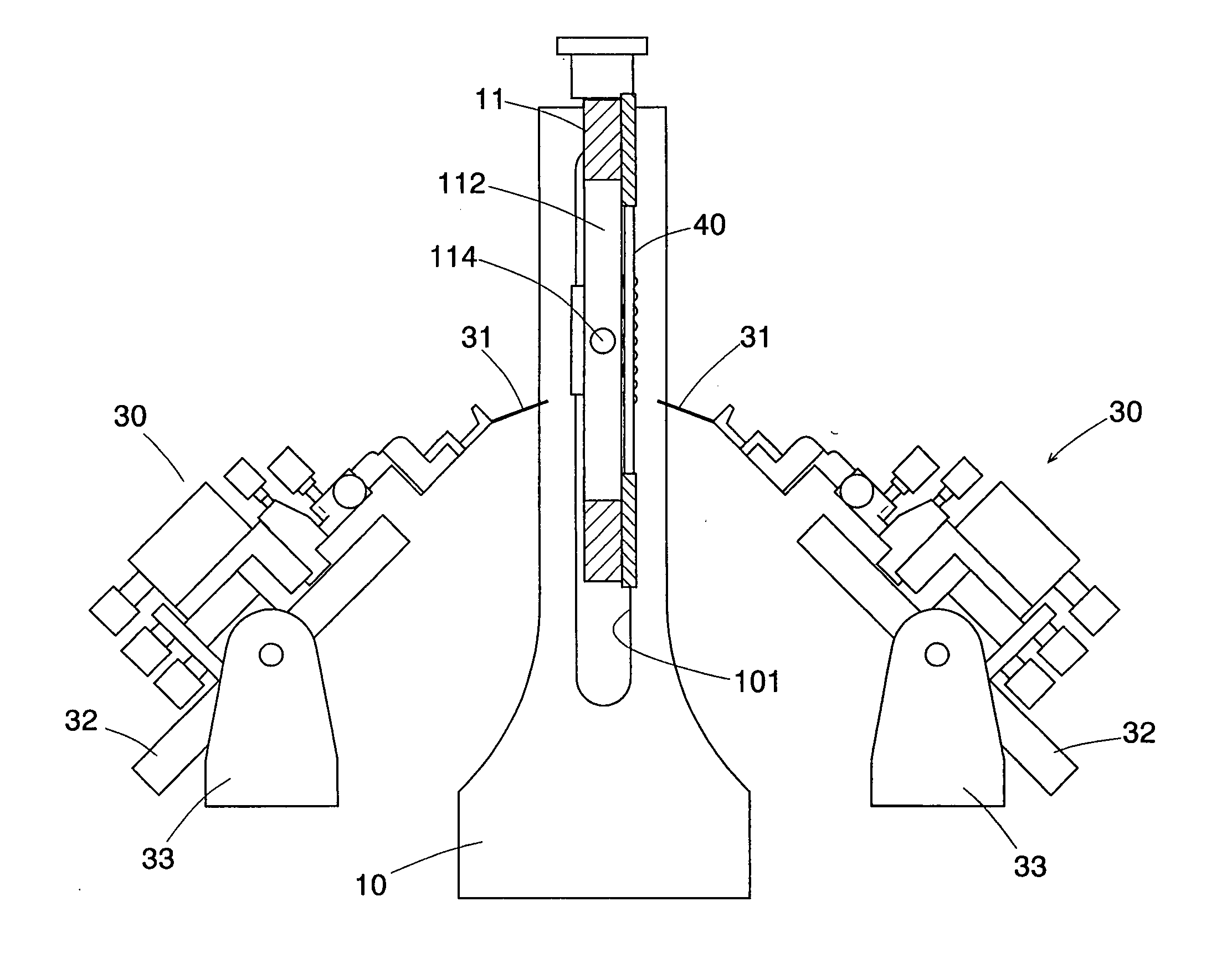
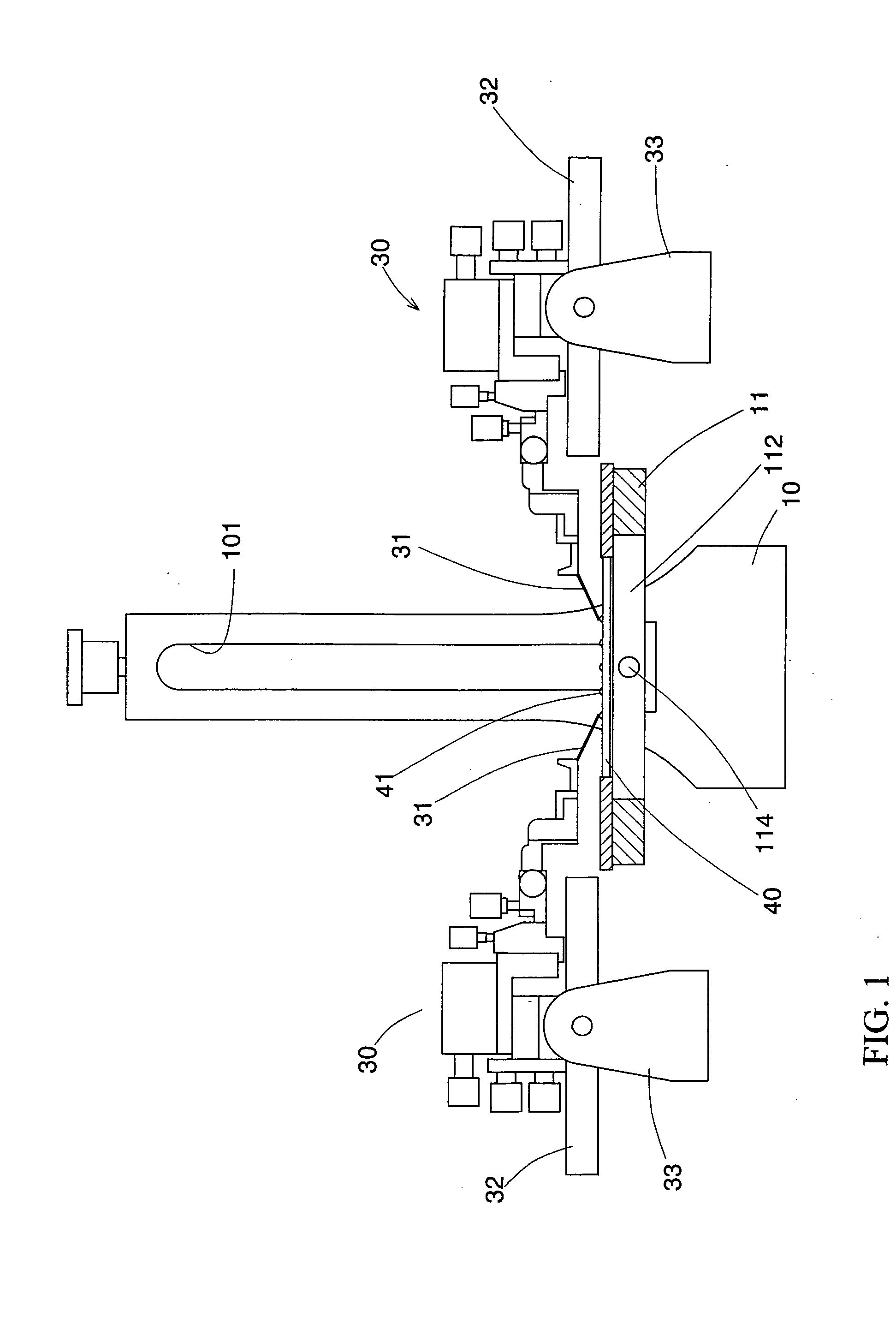
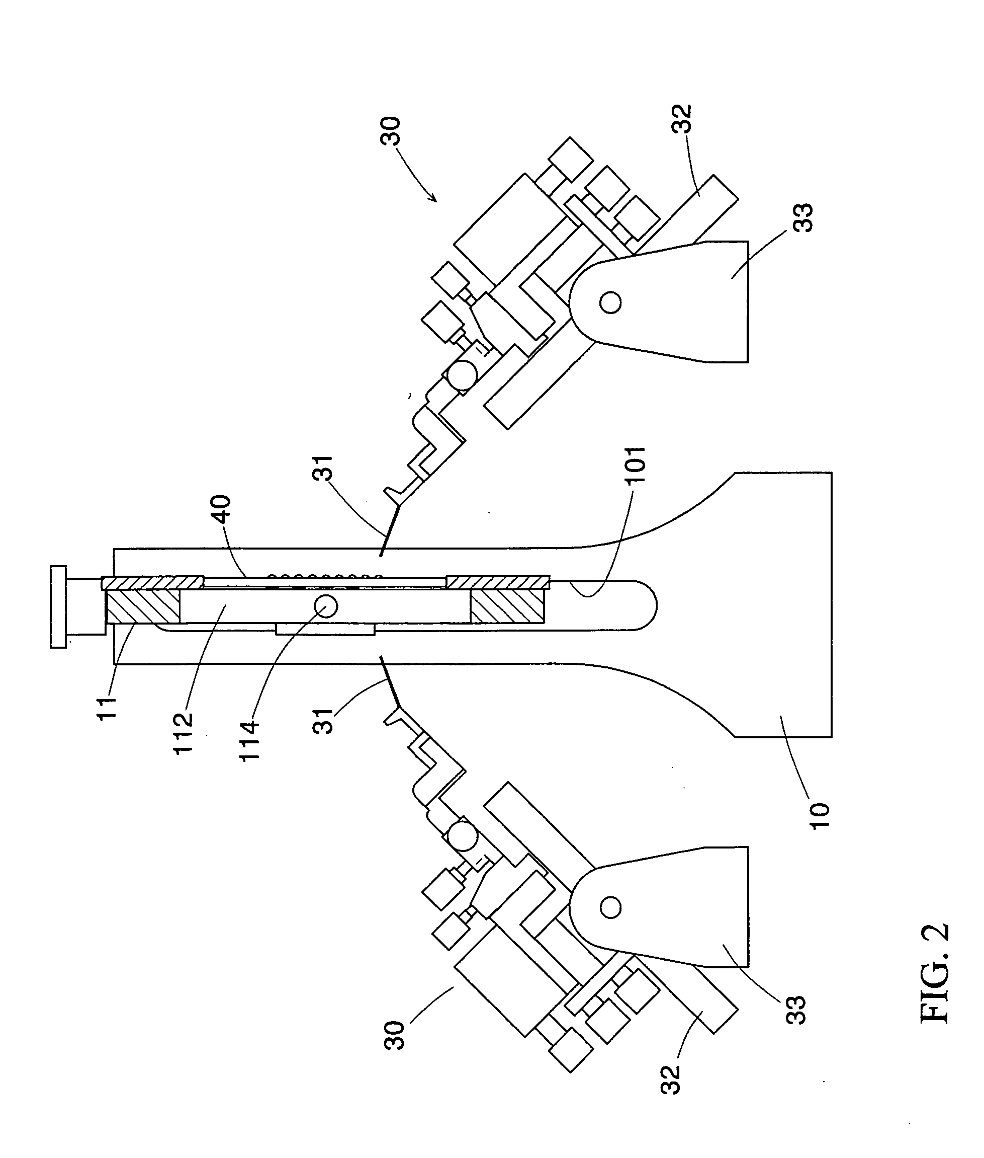
[0016] With reference to FIGS. 1 and 2, double-faced detecting devices for an electronic substrate 40 in accordance with the present invention comprises a base 10 with a substrate platform 11, two pivot bases 33, two probe-detecting machines 30 respectively mounted on the two pivot bases 33. Particularly, the electronic substrate 40 has a top face and a bottom face and multiple contacts 41 respectively arranged on the top and bottom faces.

[0017] The base 10 has an erecting post (not numbered) with a front face, an guiding groove 101 longitudinally defined in the front face of the erecting post, and the substrate platform 11 with a connecting rod 112 movably and rotatably attached to the erecting post via the guiding groove 101. The substrate platform 11 has a top face. A through hole 114 is defined in the substrate platform 11 and has a diameter smaller than that of the electronic substrate 40. Therefore, the electronic substrate 40 enables to be mounted on the top face of the subs...


PUM


Abstract

Double-faced detecting devices for an electronic substrate, the detecting device have a base and two probe-detecting machines oppositely located beside the base. The base has a guiding groove and a substrate platform with a through hole rotatably and movably mounted on the base via the guiding groove. Therefore, when the electronic substrate mounts on the substrate platform, the substrate platform enables to rotate from a horizontal position to a vertical position to expose two faces of the electronic substrate to face the two probe-detecting machines for a double-faced detection of the electronic substrate in high-frequency properties. Additionally, each probe-detecting machine is mounted on a pivot base and pivoted by the pivot base to adjust the height of probe to touch the electronic substrate at the vertical position.

Description

FIELD OF THE INVENTION [0001] In general, the present invention relates to double-faced detecting devices for an electronic substrate, and more particularly to detecting devices that enables to alternatively place the electronic substrate in a horizontal position or a vertical position to detect high-frequency properties of the electronic substrate. BACKGROUND OF THE INVENTION [0002] With reference to FIG. 5, conventional detecting devices for an electronic substrate, such as a flip chip, a wafer or a printed circuit board (PCB), in high-frequency properties comprises two opposite probe-detecting machines 50 and a substrate platform 70. Each probe-detecting machine 50 has a probe 51 secured on an inward face of the probe-detecting machine 50 and connects to a detecting system (example: networking analysis instrument) via a high-frequency isolation wire (not shown). The two probe-detecting machines 50 are respectively mounted on two bases 60. The substrate platform 70 is located betw...

Claims


Application Information

Patent Timeline
Patent Type & Authority Applications(United States)
IPC IPC(8): G01R1/067G01R31/02G01R31/28
CPCG01R1/06772G01R31/2893G01R31/2808
Inventor HSU, MING-HUEY
Owner PREMTEK INT
Why Eureka
Try Eureka