Electrolytic processing method

a processing method and electrolysis technology, applied in the direction of manufacturing tools, electric circuits, electric circuits, etc., can solve the problem that the sensor portion of the processing electrode is not capable of processing, and achieve the effect of high precision and simple construction

Inactive Publication Date: 2009-08-25
EBARA CORP
View PDF5 Cites 0 Cited by
  • Summary
  • Abstract
  • Description
  • Claims
  • Application Information

AI Technical Summary

Benefits of technology

[0013]The present invention has been made in view of the above situation in the related art. It is therefore an object of the present invention to provide an electrolytic processing apparatus and an electrolytic processing method which can detect the end point of electrolytic processing stably with high precision and with a relatively simple construction.

Problems solved by technology

In the case where the processing electrode and the feeding electrode are disposed close to each other, for example, provision of the eddy current sensor within the processing electrode will make the sensor portion of the processing electrode not capable of processing.

Method used


Image

  • Electrolytic processing method
  • Electrolytic processing method
  • Electrolytic processing method

Examples


Embodiment Construction

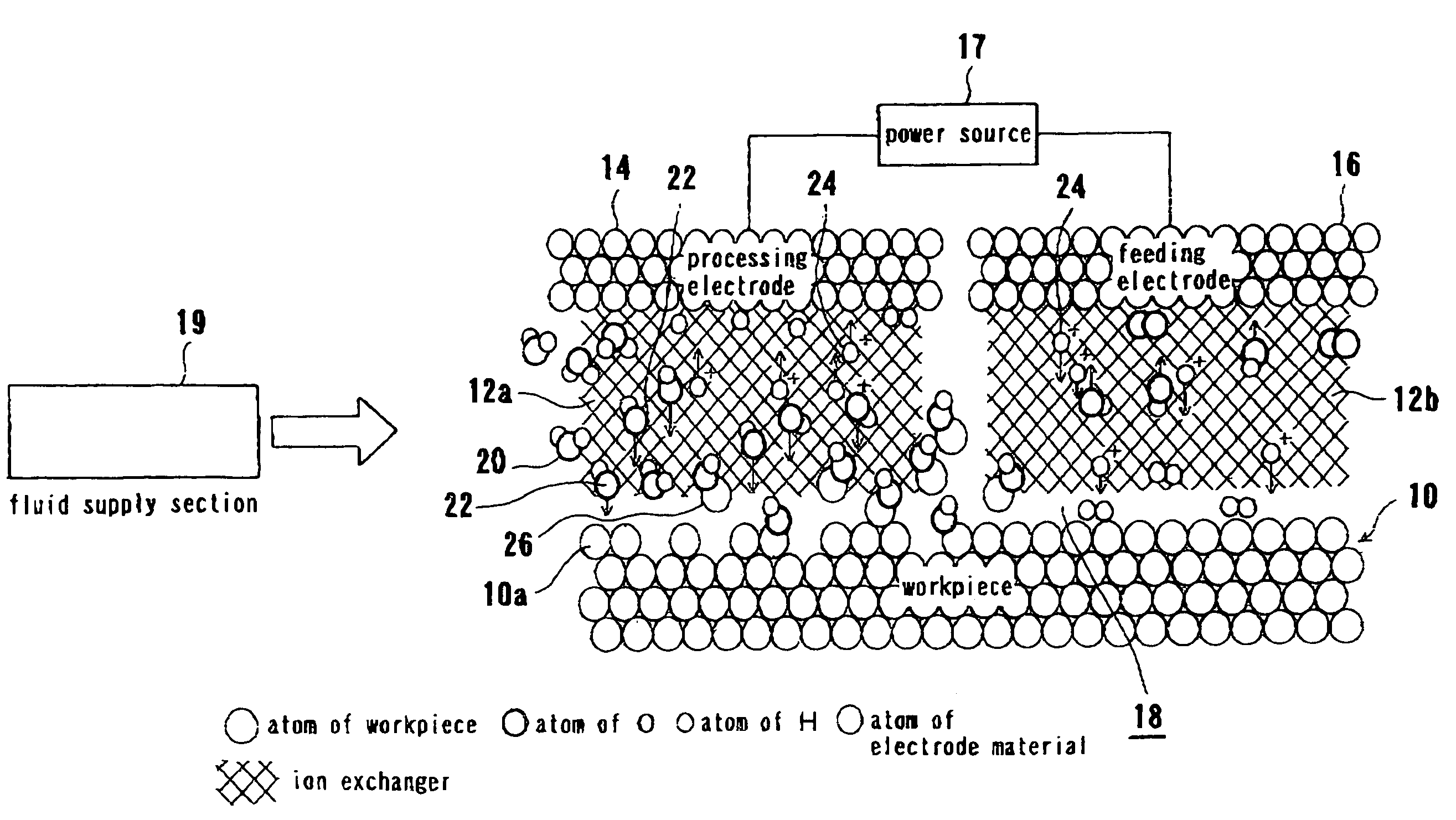
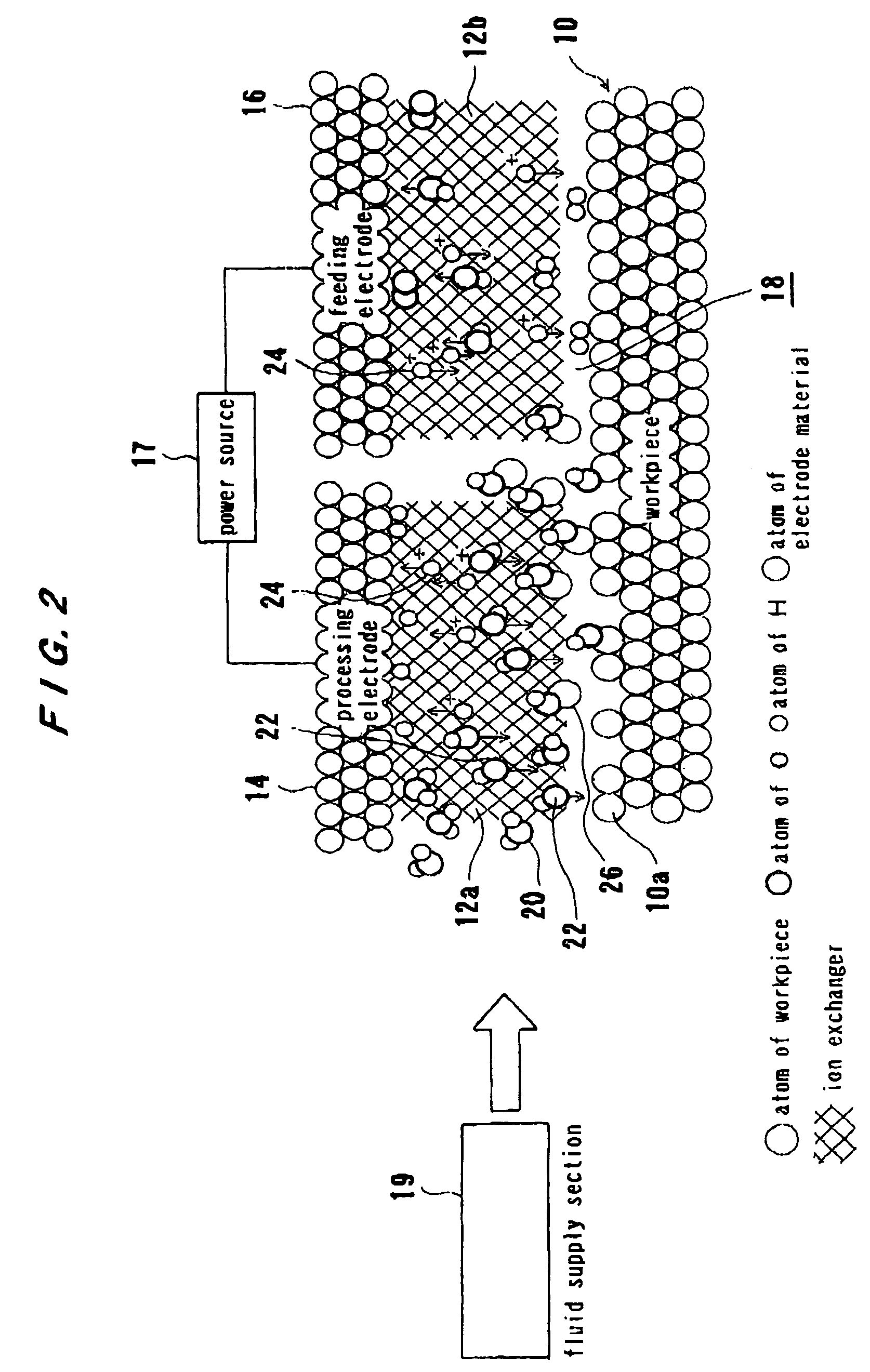
[0056]Preferred embodiments of the present invention will now be described with reference to the drawings.

[0057]FIG. 3 is a plan view illustrating the construction of a substrate processing apparatus incorporating an electrolytic processing apparatus according to an embodiment of the present invention. According to the embodiment, a conductive film, such as a copper film or a barrier layer, formed in the surface of a substrate is processed (polished) by an electrolytic processing apparatus. The present invention is of course applicable to besides the substrate.

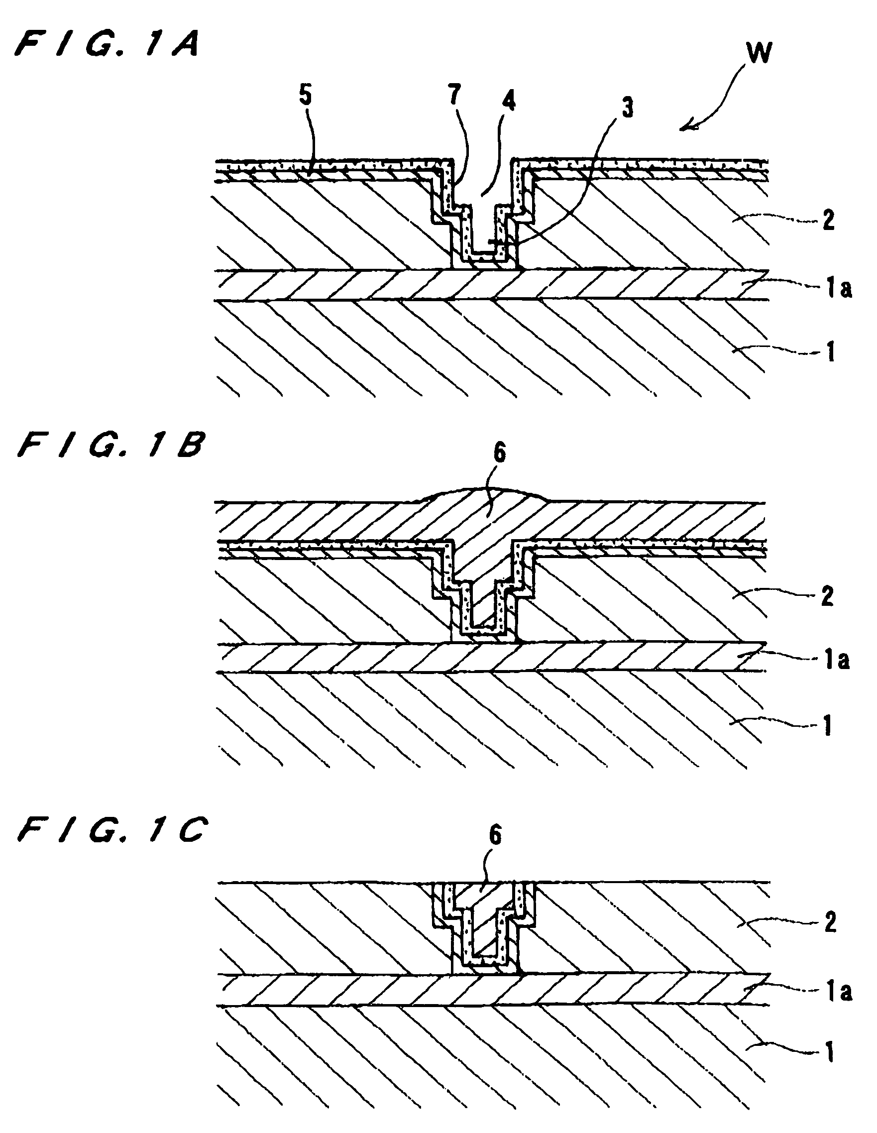
[0058]As shown in FIG. 3, the substrate processing apparatus comprises a pair of loading / unloading sections 30 as a carry-in / carry-out section for carrying in and out a substrate, e.g. a substrate W, as shown in FIG. 1B, which have a copper film 6 and a barrier layer 6 as conductive films (processing objects) in its surface, a first cleaning machine 31a for performing a primary cleaning of the substrate, a second cleaning mach...


PUM

PropertyMeasurementUnit
electric conductivityaaaaaaaaaa
porosityaaaaaaaaaa
diameteraaaaaaaaaa

Abstract

An electrolytic processing apparatus can detect the end point of electrolytic processing stably with high precision and with a relatively simple construction. The electrolytic processing apparatus includes: a processing electrode which can come close to or into contact with a processing object; a feeding electrode for feeding electricity to the processing object; a fluid supply section for supplying fluid between the processing object and at least one of the processing electrode and the feeding electrode; a processing power source for applying a voltage between the processing electrode and the feeding electrode; a drive section for causing relative movement between the processing object and at least one of the processing electrode and the feeding electrode; and an eddy current sensor for detecting the thickness of the processing object from a change in eddy current loss. The sensor is disposed not in contact with (or separately) by an insulator from the processing electrode and / or the feeding electrode.

Description

BACKGROUND OF THE INVENTION[0001]1. Field of the Invention[0002]The present invention relates to an electrolytic processing apparatus and an electrolytic processing method, and more particularly to an electrolytic processing apparatus and an electrolytic processing method useful for processing a conductive material in a surface of a substrate, such as a semiconductor wafer, or for removing impurities adhering to a surface of a substrate.[0003]2. Description of the Related Art[0004]In recent years, instead of using aluminum or aluminum alloys as a material for forming circuits on a substrate such as a semiconductor wafer, there is an eminent movement towards using copper (Cu) which has a low electric resistivity and high electromigration resistance. Copper interconnects are generally formed by filling copper into fine recesses formed in the surface of a substrate. There are known various techniques for forming such copper interconnects, including chemical vapor deposition (CVD), sput...

Claims


Application Information

Patent Timeline
Patent Type & Authority Patents(United States)
IPC IPC(8): C25D21/12C25F3/02C25C7/06C25F7/00
CPCC25F7/00
Inventor NOJI, IKUTAROYASUDA, HOZUMIIIZUMI, TAKESHIHIROKAWA, KAZUTOKOBATA, ITSUKI
Owner EBARA CORP
Why Eureka
Try Eureka