Apparatus having line source of radiant energy for exposing a substrate

a radiant energy and apparatus technology, applied in the direction of photomechanical apparatus, instruments, manufacturing tools, etc., can solve the problems of expensive lasers, difficult to achieve good dose uniformity over a relatively large area in a single, and large area

Inactive Publication Date: 2003-03-11
VEECO INSTR
View PDF11 Cites 269 Cited by
  • Summary
  • Abstract
  • Description
  • Claims
  • Application Information

AI Technical Summary

Problems solved by technology

Because the required field size can exceed four (4) centimeters-squared (cm.sup.2) and the required dose can exceed one (1.0) Joules / cm.sup.2, a relatively large, expensive laser is required.
It is also difficult to achieve good dose uniformity over a relatively large area in a single pulse because the narrow spectral range of most lasers produces a speckled pattern due to interference effects.

Method used


Image

  • Apparatus having line source of radiant energy for exposing a substrate
  • Apparatus having line source of radiant energy for exposing a substrate
  • Apparatus having line source of radiant energy for exposing a substrate

Examples


first embodiment

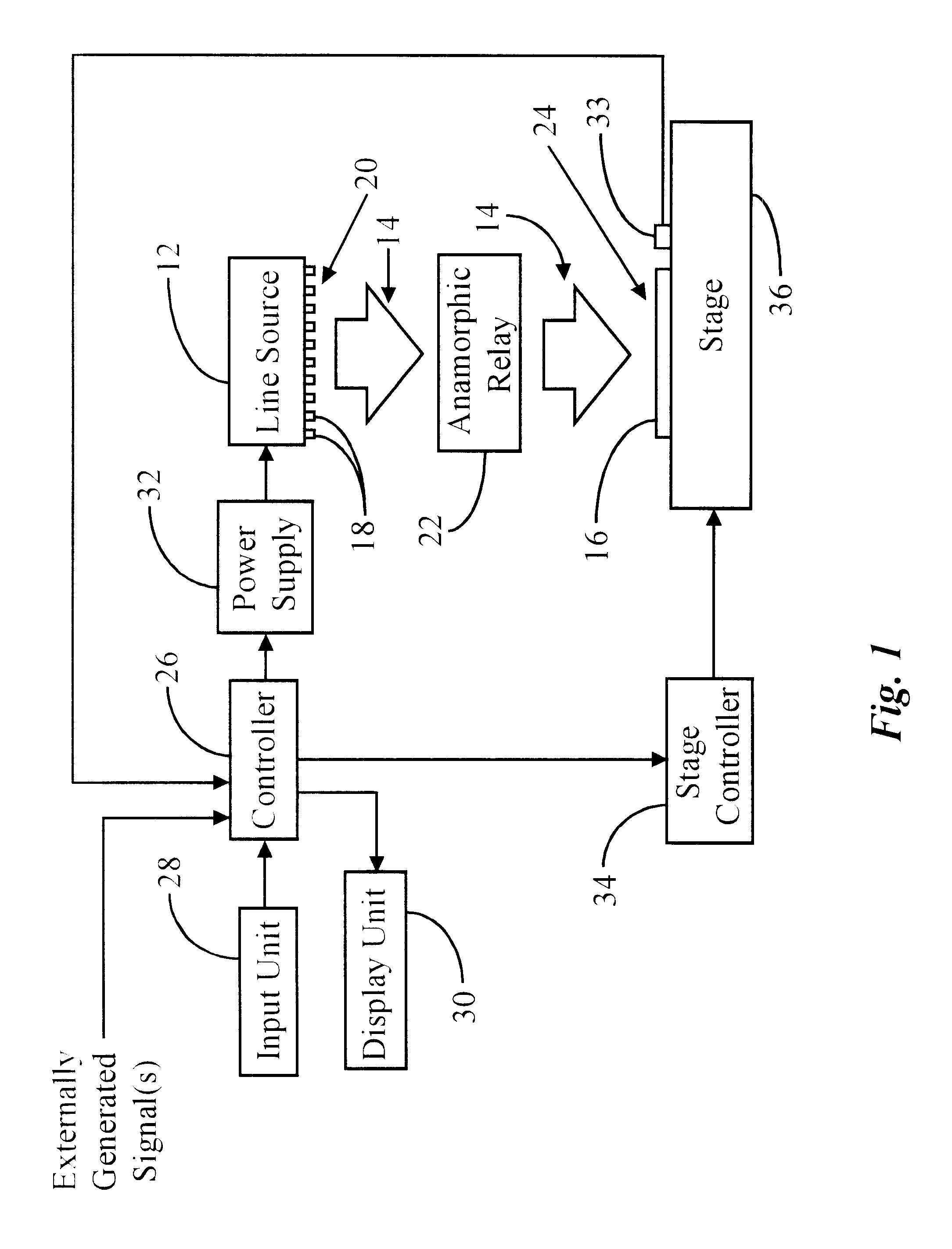
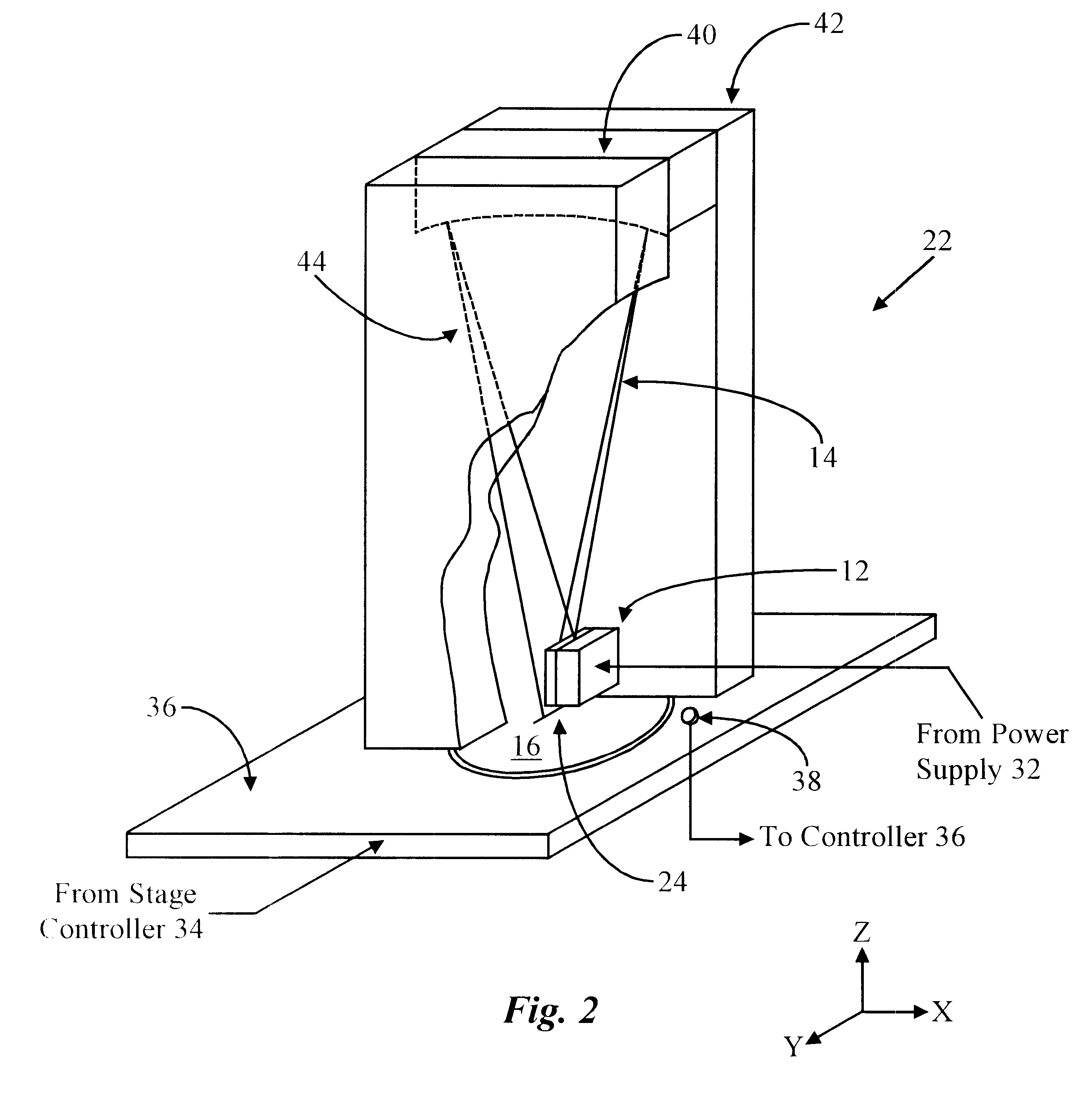
In FIG. 1, an apparatus 10 in accordance with this invention is shown. The apparatus 10 includes a line source 12 that generates relatively intense radiant energy 14 used for treatment of a substrate 16. The line source 12 includes one or more laser diode arrays each having a plurality of laser diodes 18 positioned at regular spaced intervals along a linear emission face 20 thereof. The laser diodes 18 are relatively closely-spaced and positioned at intervals along a linear direction defining the axis of the laser diode array. The line source 12 can generate radiant energy 14 at a wavelength from about 350 nanometers (nm) to 950 nm. Such wavelength range is particularly effective for processing the substrate 16 if such substrate is composed of silicon and the integrated device or circuit features are on the order of one micron or less with source / drain regions of a few. tens of nanometers (nm). in thickness. However, the invented apparatus is not limited to a line source 12 that gen...

second embodiment

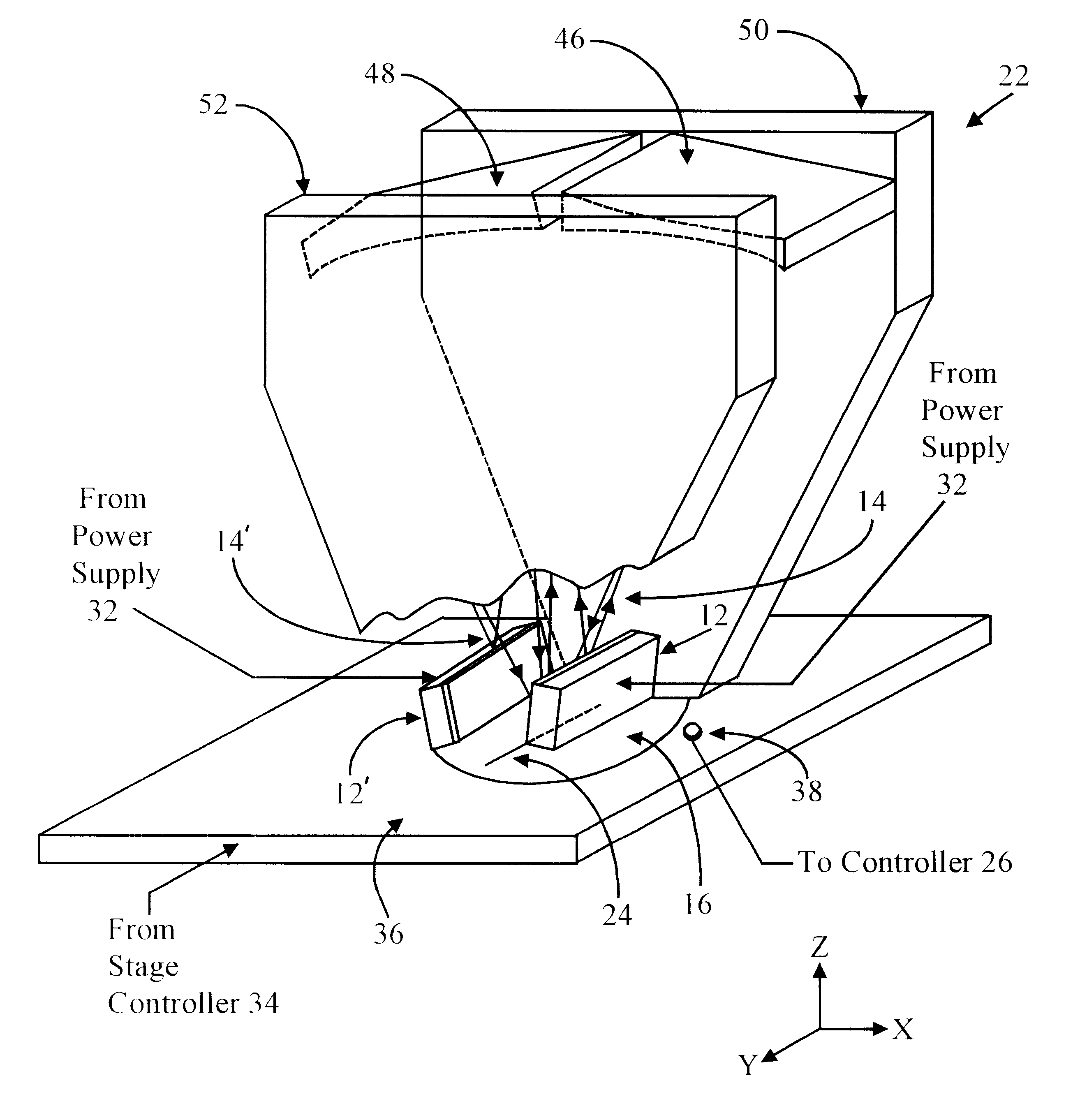
In FIG. 6, the apparatus 10 is shown. The apparatus 10 includes an additional line source 12' that can include laser diode array(s). Like the line source 12, the line source 12' is coupled to receive current from the power supply 32. Based on the current, the line source 12' generates radiant energy 14'. The relay 22 includes elliptical or spherical mirrors 46, 48, and planar side wall mirrors 50, 52. The line source 12 is arranged to direct radiant energy 14 to the mirror 46, which reflects such radiant energy to the line image 24. Similarly, the line source 12' is arranged to direct radiant energy 14' to the mirror 48, which also reflects such radiant energy to the line image 24. The relay 22 images the line sources 12, 12' to the same position or adjacent positions to form the line image 24. The side wall mirrors 50, 52 are positioned on opposite sides of the mirrors 46, 48 and are preferably spaced apart a distance equal to the length. of the line image 24. The mirrors 50, 52 re...

sixth embodiment

In FIG. 11, the optical relay 22 in the apparatus 10 is catoptric, i.e., all-reflective, non-refractive. The optical relay 22 of FIG. 11 includes a mirror 104 with a base 106 defining intersecting planar reflective surfaces 108, 110. The base 106 includes a rigid material such as glass or plastic, that defines the surfaces 108, 110. The surfaces 108, 110 are made reflective by deposition of reflective material(s) such as aluminum or alternating dielectric layers of different refractive indices on such surfaces. The line source 12 is arranged to direct radiant energy 14 to the reflective surface 108, and the line source 12' is arranged to direct radiant energy 14' to the reflective surface 110. The radiant energy 14, 14' reflected from respective surfaces 108, 110 travels to respective portions of the reflective surface of the curved mirror 111. The radiant energy 14, 14' reflected from the mirror 111 travels to the substrate 16 to form the image 24 thereon. As shown in FIG. 11, the ...


PUM

PropertyMeasurementUnit
wavelengthaaaaaaaaaa
wavelength rangeaaaaaaaaaa
wavelengthsaaaaaaaaaa

Abstract

Radiant energy line source(s) (e.g., laser diode array) and anamorphic relay receiving radiant energy therefrom and directing that energy to a substrate in a relatively uniform line image. The line image is scanned with respect to the substrate for treatment thereof. Good uniformity is provided even when the line source is uneven. Optionally, delimiting aperture(s) located in the anamorphic relay focal plane and a subsequent imaging relay are includeable to permit substrate exposure in strips with boundaries between adjacent strips within scribe lines between circuits. An anamorphic relay focal plane mask with a predetermined pattern can be used to define portions of the substrate to be treated with the substrate and mask scanning motions synchronized with each other. Control of source output, and position/speed of the substrate, with respect to the line image, allows uniform dose and required magnitude over the substrate.

Description

1. Field of the InventionThis invention is directed to an apparatus and method that generates radiant energy for use in processing a substrate and / or integrated devices or circuits formed thereon. For example, the apparatus and method can be used to supply radiant energy to anneal and / or activate dopants of source, drain or gate regions of integrated devices or circuits, to form silicide regions in integrated devices or circuits to lower contact resistances of metal wiring coupled thereto, or to trigger a chemical reaction to either form or remove substances from a substrate. The invented apparatus and method can also be used to generate, pattern, and direct radiant energy to a substrate for selective treatment thereof.2. Description of the Related ArtVarious devices for laser treatment of semiconductor substrates have been known and used in the integrated circuit fabrication industry. Laser annealing is preferably done in a single cycle that brings the temperature of the material t...

Claims


Application Information

Patent Timeline
Patent Type & Authority Patents(United States)
IPC IPC(8): B23K26/06B23K26/073G03F7/20H01L21/00H01L21/20H01L21/268
CPCB23K26/0738G03F7/70225G03F7/70558G03F7/70391H01L21/67115H01L21/027
Inventor MARKLE, DAVID A.HAWRYLUK, ANDREW M.JEONG, HWAN J.
Owner VEECO INSTR
Why Eureka
Try Eureka