Offset-bonded, multi-chip semiconductor device

a semiconductor device and chip technology, applied in semiconductor devices, semiconductor/solid-state device details, electrical devices, etc., can solve the problems of affecting the reliability of bonding, affecting the bonding reliability of the bonding, and affecting the placement of external connection terminals

Inactive Publication Date: 2005-06-09
RENESAS ELECTRONICS CORP
View PDF8 Cites 40 Cited by
  • Summary
  • Abstract
  • Description
  • Claims
  • Application Information

AI Technical Summary

Benefits of technology

[0017] According to this configuration, the load of the upper second semiconductor element can act only as a pressing force which pressurizes the bumps between the first semiconductor element and second semiconductor element, and never exerts tensile force to the bumps. For the case where the upper second semiconductor element is shifted with respect to the lower first semiconductor element to thereby produce the external connection terminal region on the first semiconductor element, this configuration makes it possible to keep a high reliability of bonding through the bumps between the first semiconductor element and second semiconductor element.
[0033] The semiconductor device is also configured as having a first semiconductor element and a second semiconductor element stacked thereon, while allowing one end face of the second semiconductor element to run over at least one end face of the first semiconductor element; disposing a dummy chip under the run-over region of the second semiconductor element, bonding the second semiconductor element to the dummy chip through the bumps; and allowing the center of gravity of the second semiconductor element to fall inside a region having a maximized area which is determined by connecting the outermost bumps in a first bump area and the outermost bumps in a second bump area so as to include the entire portions of the individual bump areas, where the first bump area is surrounded by the outermost bumps bonding the first semiconductor element and the second semiconductor element, and the second bump area is surrounded by the outermost bumps bonding the second semiconductor element and the dummy chip. This configuration makes it possible to ensure the mechanical strength and to improve reliability in the electrical bonding, even when the center of gravity of the second semiconductor element falls outside the region surrounded by the bumps between the first semiconductor element and second semiconductor element.

Problems solved by technology

In the above-described case, the main chip surface of the lower first LSI chip does not expose outside the upper second LSI chip, and this makes it impossible to arrange the external connection terminals interfaced with the external, on the circumferential portion of the main chip surface.
The stress may result in breakage of the bumps 63 between the upper and lower chips, to thereby degrade the bonding reliability.

Method used


Image

  • Offset-bonded, multi-chip semiconductor device
  • Offset-bonded, multi-chip semiconductor device
  • Offset-bonded, multi-chip semiconductor device

Examples


first embodiment

[0053] (First Embodiment)

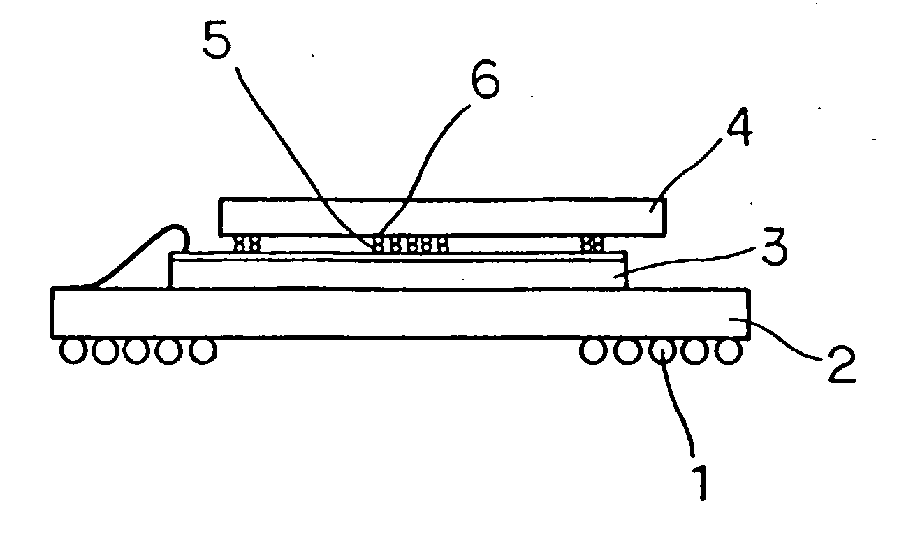
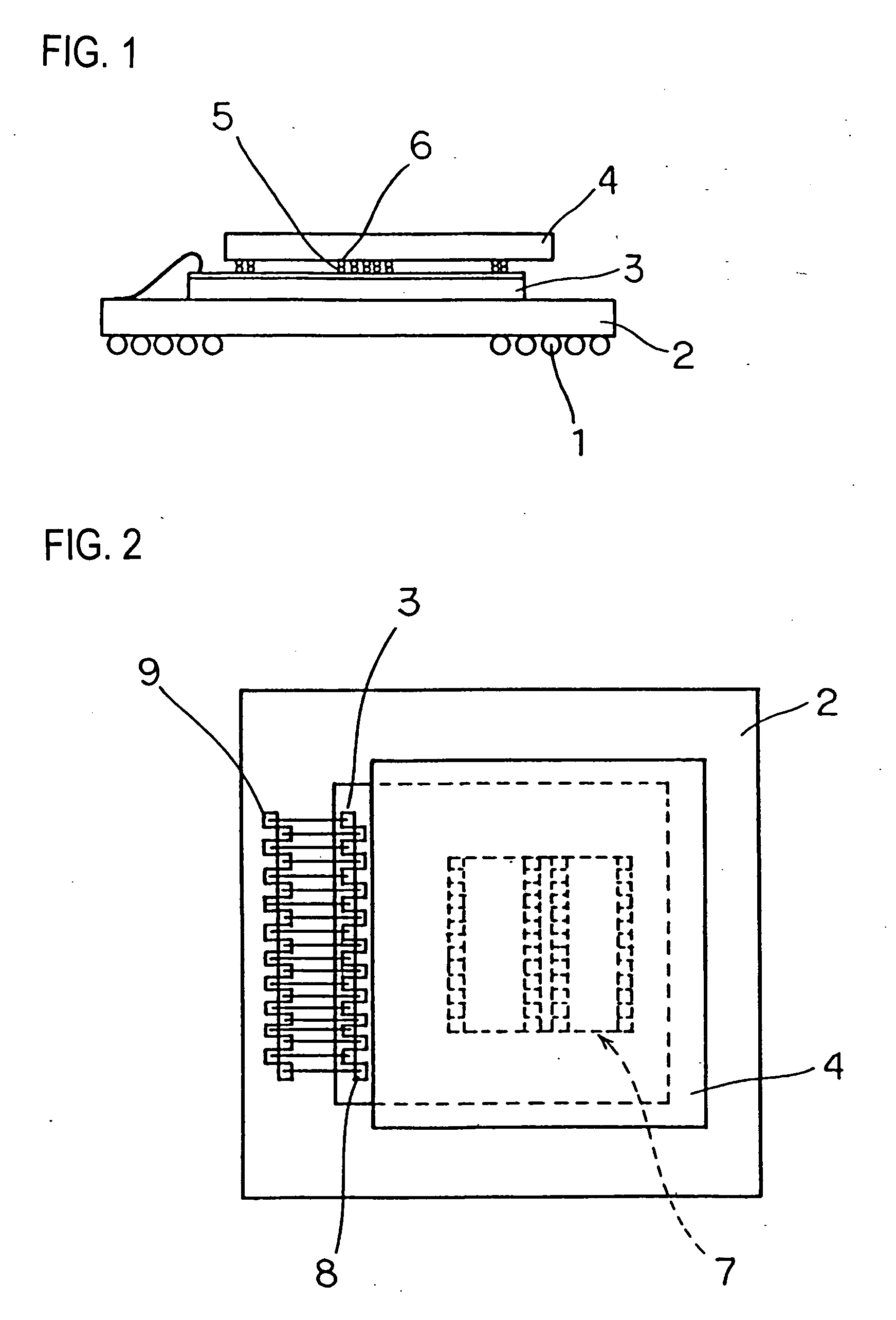
[0054]FIG. 1 is a side elevation showing a configuration of a COC-type semiconductor device according to the first embodiment of the present invention, and FIG. 2 is a plan view of the semiconductor device shown in FIG. 1.

[0055] Referring now to FIG. 1, ball bumps 1 as electrode terminals are arranged on one surface of a substrate (printed wiring board, for example) 2 having electric wirings already formed thereon. On the other surface of the substrate 2, a first chip 3 is mounted. The first chip 3 and a second chip 4 are bonded with each other so that the second chip 4 is shifted in parallel from the first chip 3, while allowing a portion of the second chip 4 to run over the first chip 3.

[0056] The first chip 3 disposed on the lower side is a logic chip, and the second chip 4 is a memory chip having a larger geometrical area than that of the logic chip. The first chip 3 can be a silicon chip.

[0057] The first chip 3 and second chip 4 are bonded based on t...

second embodiment

[0084] (Second Embodiment)

[0085] The first embodiment exemplified the semiconductor device having two chips stacked on the substrate, but the present embodiment will exemplify a semiconductor device having three or more chips stacked on a substrate.

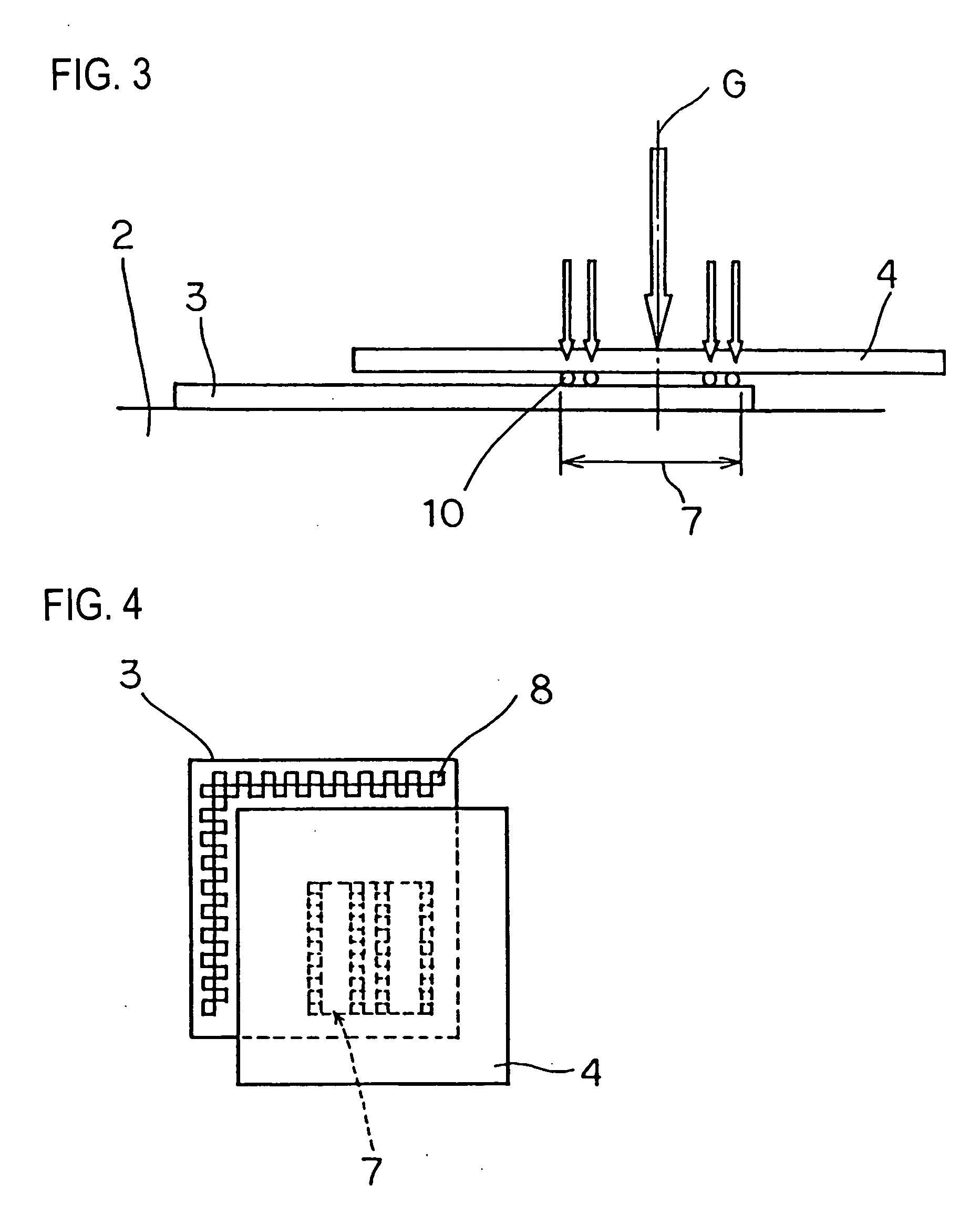
[0086]FIG. 14 and FIG. 15 are side elevations of semiconductor devices according to the second embodiment of the present invention, respectively having a plurality of chips stacked therein.

[0087]FIG. 14 shows an embodiment of a semiconductor device having three chips stacked on a substrate.

[0088] Similarly to the first embodiment, the first chip 3 is mounted on the substrate having electric wirings already formed thereon, and the second chip 4 is bonded on the first chip 3 based on the face-down bonding style. Parallel shifting of the second chip 4 with respect to the first chip 3 allows the surface of the first chip 3 to expose, and the exposed region serves as the external connection terminal region having a plurality of bonding pad ...


PUM


Abstract

The present invention is aimed at bonding a lower chip and an upper chip through bumps in a highly reliable manner, while ensuring a sufficient area for an external connection terminal region, by offsetting the upper chip to the lower chip. The substrate 2 has bumps 1 arranged on one surface thereof, and has a first chip 3 mounted on the other surface thereof. A second chip 4 is bonded to the first chip 3 through bumps 5, 6 while offsetting the second chip 4 to the first chip 3 in parallel. In the bonded state of the first chip 3 and the second chip 4, a part of the first chip 3 and a part of the second chip 4 are overlapped without aligning the centers of the both. The center of gravity of the second chip 4 falls inside a region surrounded by the outermost bumps between the first chip 3 and the second chip 4.

Description

[0001] This application is based on Japanese patent applications No. 2003-400105 and No. 2004-317903, the contents of which are incorporated hereinto by reference. DISCLOSURE OF THE INVENTION [0002] 1. Field of the Invention [0003] The present invention relates to a semiconductor device having a mounting unit which comprises semiconductor elements (referred to as “chips”, hereinafter) having electrodes formed on the individual surfaces, being bonded so as to be offset to each other and so as to oppose the surfaces thereof, and in particular to a offset-bonded, multi-chip semiconductor device in which two or more semiconductor elements are stacked and bonded. [0004] 2. Related Art [0005] For the purpose of reducing both of cost and size of semiconductor integrated circuit device, there is proposed a COC (Chip On Chip)-type semiconductor device in which two LSI chips are bonded with each other based on the face-down bonding style, to thereby form a mounting unit. [0006] A conventional...

Claims


Application Information

Patent Timeline
Patent Type & Authority Applications(United States)
IPC IPC(8): H01L25/18H01L23/50H01L25/00H01L25/065H01L25/07H01L29/40
CPCH01L24/73H01L2924/10253H01L2224/48091H01L2224/48227H01L2224/48247H01L2225/0651H01L2225/06513H01L2225/06555H01L2225/06562H01L2225/06593H01L2924/01029H01L2924/01033H01L2924/01073H01L2924/01079H01L2924/01082H01L2924/15311H01L25/0657H01L2224/92247H01L2224/73265H01L2224/32245H01L2224/32225H01L2224/32145H01L2224/16145H01L2924/10329H01L2924/01074H01L2924/01068H01L2924/01024H01L2924/01006H01L2924/01005H01L2924/00014H01L2924/00012H01L2924/00H01L2924/14H01L2924/181
Inventor KAWANO, MASAYAMATSUI, SATOSHI
Owner RENESAS ELECTRONICS CORP
Why Eureka
Try Eureka