Power module and method of manufacturing power module
Active Publication Date: 2016-10-13
MITSUBISHI ELECTRIC CORP
View PDF6 Cites 13 Cited by
Summary
Abstract
Description
Claims
Application Information
AI Technical Summary
This helps you quickly interpret patents by identifying the three key elements:
Problems solved by technology
Method used
Benefits of technology
Benefits of technology
The invention provides a structure that reduces stress at the joint between a conductor portion and a base portion, by allowing the interconnect portion to flex and absorb strain caused by differences in expansion coefficients. This results in a power module with improved reliability.
Problems solved by technology
However, due to limitation of the size of the power semiconductor device, the number of wires which can be mounted is limited, and there has been a problem that a power module for higher current is difficult to obtain.
However, in the case of the direct lead bonding, stress caused by a difference in linear expansion coefficient between the power semiconductor device and the plate-shaped main terminal is exerted on the solder portion which is a joint material, to thereby cause cracks in the solder, resulting in a problem that the reliability is deteriorated.
Method used
Image
Click on the blue label to locate the original text in one second.
Reading with bidirectional positioning of images and text.
Examples
first embodiment
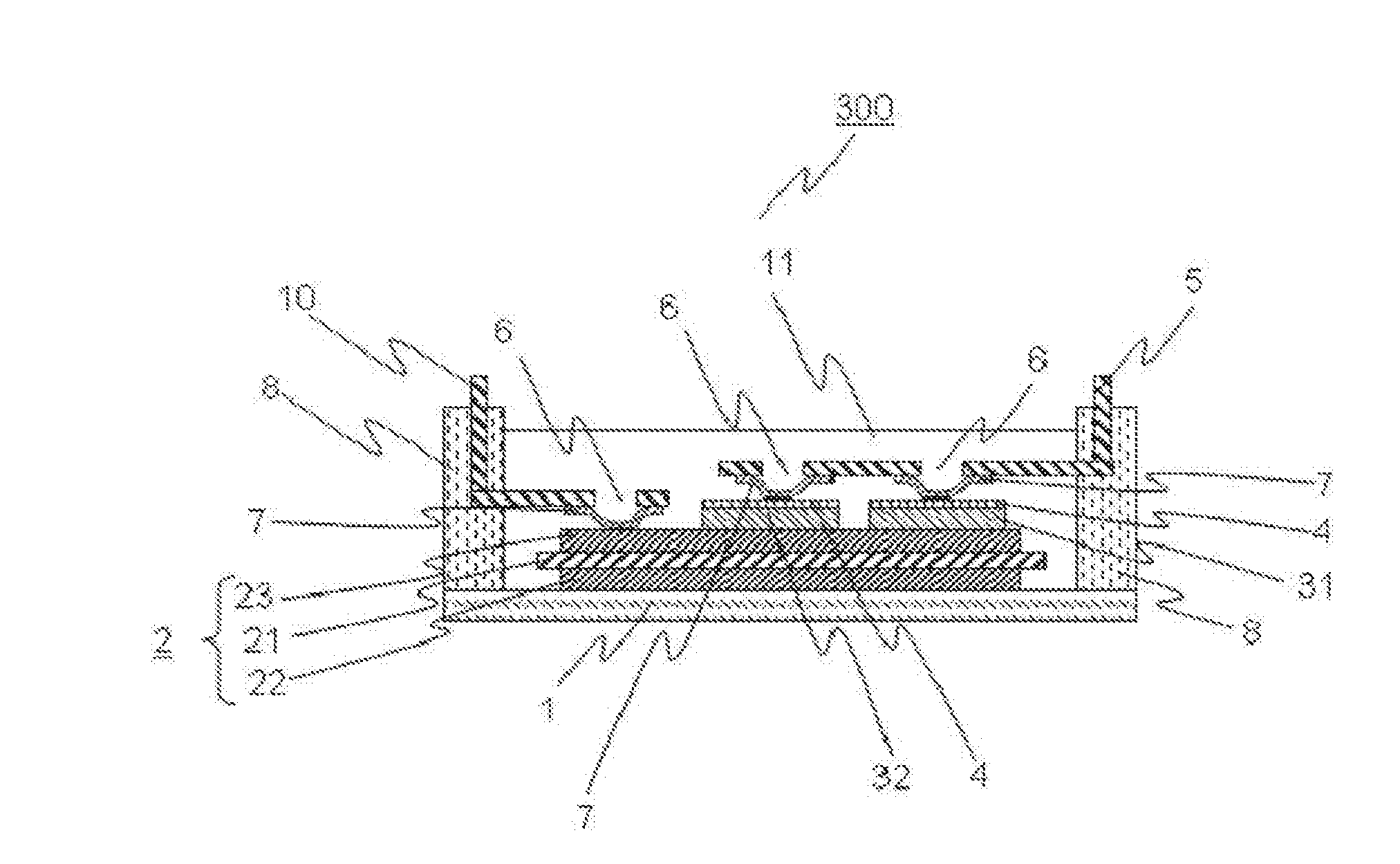
[0025]FIG. 1 is a schematic cross-sectional structure diagram of a power module in a first embodiment of the present invention. Power module 100 in FIG. 1 includes a heat-dissipation metal base plate 1, an insulating substrate 2 which is a first base portion, a power semiconductor device 3 which is a second base portion, a surface electrode 4, main terminals 5, 10 which are each a conductor portion, an opening 6, a bonding ribbon 7 which is an interconnect portion, a case 8, and a sealant resin 11.
[0026]Insulating substrate 2 is joined onto heat-dissipation metal base plate 1 with solder or the like (not shown). Insulating substrate 2 includes an insulating layer 21 and metal plates 22, 23. Insulating substrate 2 has a structure in which metal plates 22, 23 of copper or the like are bonded to respective opposite sides of insulating layer 21 formed of a ceramic material such as aluminum oxide, aluminum nitride, or siliconnitride, or formed of epoxy resin or the like. On the front-si...
second embodiment
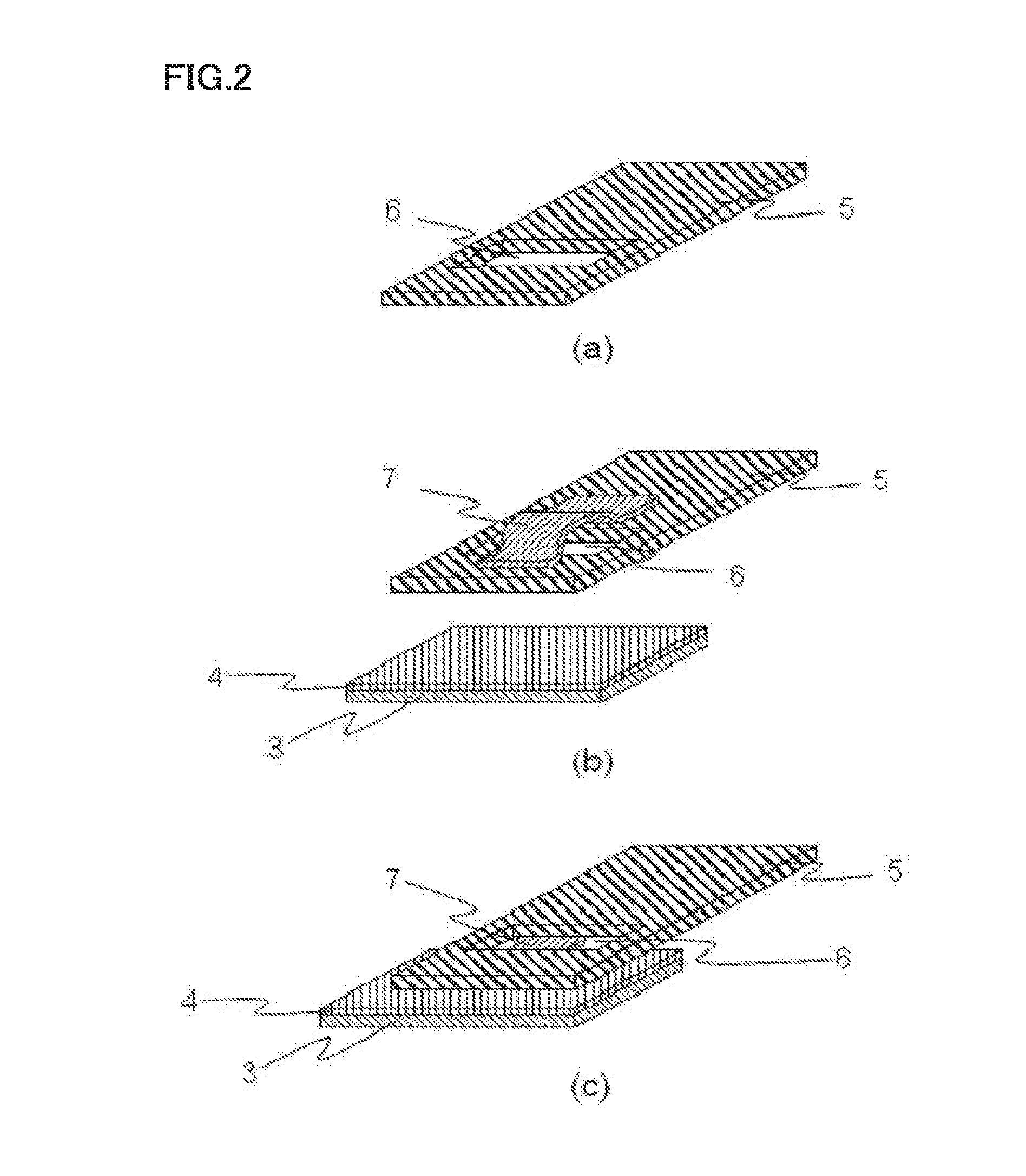
[0040]A second embodiment differs from the first embodiment in that, while main terminal 5 used in the first embodiment has opening 6, main terminal 5 of the second embodiment does not have opening 6, and in that one end of bonding ribbon 7 is ultrasonically welded to the surface of main terminal 5 facing power semiconductor device 3 and the other end of bonding ribbon 7 is ultrasonically welded to surface electrode 4 of power semiconductor device 3 in the second embodiment. Thus, the distance across which bonding ribbon 7 joins main terminal 5 to surface electrode 4 is short, and therefore, the amount of bonding ribbon 7 used for joining can be reduced.
[0041]FIG. 4 is a schematic cross-sectional structure diagram of an electrode portion of a power module in the second embodiment of the present invention. In FIG. 4, a joint portion between power semiconductor device 3 and main terminal 5 includes power semiconductor device 3, surface electrode 4, main terminal 5, and bonding ribbon ...
third embodiment
[0046]A third embodiment differs from the first embodiment in that, while solder joining is used for the joint portion between main terminal 10 and insulating substrate 2 in the first embodiment, opening 6 is formed in main terminal 10 like main terminal 5 and main terminal 10 is joined to insulating substrate 2 via bonding ribbon 7 in the third embodiment. Thus, the joint for main terminal 5 and the joint for main terminal 10 can be formed in the same step and the number of steps can be reduced. Moreover, the reliability of the joint between main terminal 10 and insulating substrate 2 can be improved.
[0047]FIG. 6 is a schematic cross-sectional structure diagram of a power module in the third embodiment of the present invention. Power module 200 in FIG. 6 includes heat-dissipation metal base plate 1, insulating substrate 2, power semiconductor device 3, surface electrode 4, main terminals 5, 10, opening 6, bonding ribbon 7, case 8, and sealant resin 11. While main terminal 10 is joi...
PUM
Abstract
A power module providing an improved manufacture yield and having an ensured stable joint strength and accordingly improved reliability is provided. The power module includes: a base portion having one surface on which an electrode portion is formed; a conductor portion disposed to face the one surface of the base portion on which the electrode portion is formed, for making electrical connection with the outside; and an interconnect portion connected to the electrode portion formed on the one surface of the base portion and to the surface of the conductor portion facing the one surface of the base portion for electrically connecting the electrode portion to the conductor portion.
Description
TECHNICAL FIELD[0001]The present invention relates to a power module, and particularly relates to an interconnect structure and a package structure of a power module.BACKGROUND ART[0002]A power module which includes a power semiconductor device (for example, IGBT (Insulated Gate Bipolar Transistor), MOSFET (MetalOxideSemiconductorField EffectTransistor), bipolar transistor, diode, or the like) mounted on a circuit board and which is packaged with a sealant resin is used for example in a motor drive apparatus or the like.[0003]A package structure called case structure is mainly used for the power module. This case-type structure is a structure in which a power semiconductor device is mounted on a heat-dissipation metal base plate with an insulating substrate interposed therebetween and a case is bonded to the heat-dissipation metal base plate.[0004]The power semiconductor device mounted in the module is connected to a main electrode. For connecting the power semiconductor device ...
Claims
Application Information
Patent Timeline
Application Date:The date an application was filed.
Publication Date:The date a patent or application was officially published.
First Publication Date:The earliest publication date of a patent with the same application number.
Issue Date:Publication date of the patent grant document.
PCT Entry Date:The Entry date of PCT National Phase.
Estimated Expiry Date:The statutory expiry date of a patent right according to the Patent Law, and it is the longest term of protection that the patent right can achieve without the termination of the patent right due to other reasons(Term extension factor has been taken into account ).
Invalid Date:Actual expiry date is based on effective date or publication date of legal transaction data of invalid patent.

