Duplexing wiring layer and its circuit structure

A technology for rewiring layers and circuit structures, applied in the structural field of multi-layer metal layers, which can solve problems such as cracks, delamination, and inconvenience

Inactive Publication Date: 2006-11-01
ADVANCED SEMICON ENG INC
View PDF0 Cites 13 Cited by
  • Summary
  • Abstract
  • Description
  • Claims
  • Application Information

AI Technical Summary

Problems solved by technology

[0005] It is worth noting that the existing conventional redistribution layer 120 has poor bonding between the circuit layer 124 and the dielectric layers 122, 126, which may easily cause cracks on the bonding surface under the solder bump 132, and the circuit The phenomenon of delamination (peeling) will also occur between the layer 124 and the two adjacent dielectric layers 122 and 126 due to poor bonding, which affects the reliability of the chip package.
[0006] It can be seen that the above-mentioned existing redistributi

Method used


Image

  • Duplexing wiring layer and its circuit structure
  • Duplexing wiring layer and its circuit structure

Examples


Embodiment Construction

[0042] In order to further explain the technical means and effects of the present invention to achieve the intended purpose of the invention, the specific implementation, structure, and characteristics of the redistribution layer and its circuit structure proposed according to the present invention will be described below in conjunction with the accompanying drawings and preferred embodiments. And its effect, detailed description is as follows.

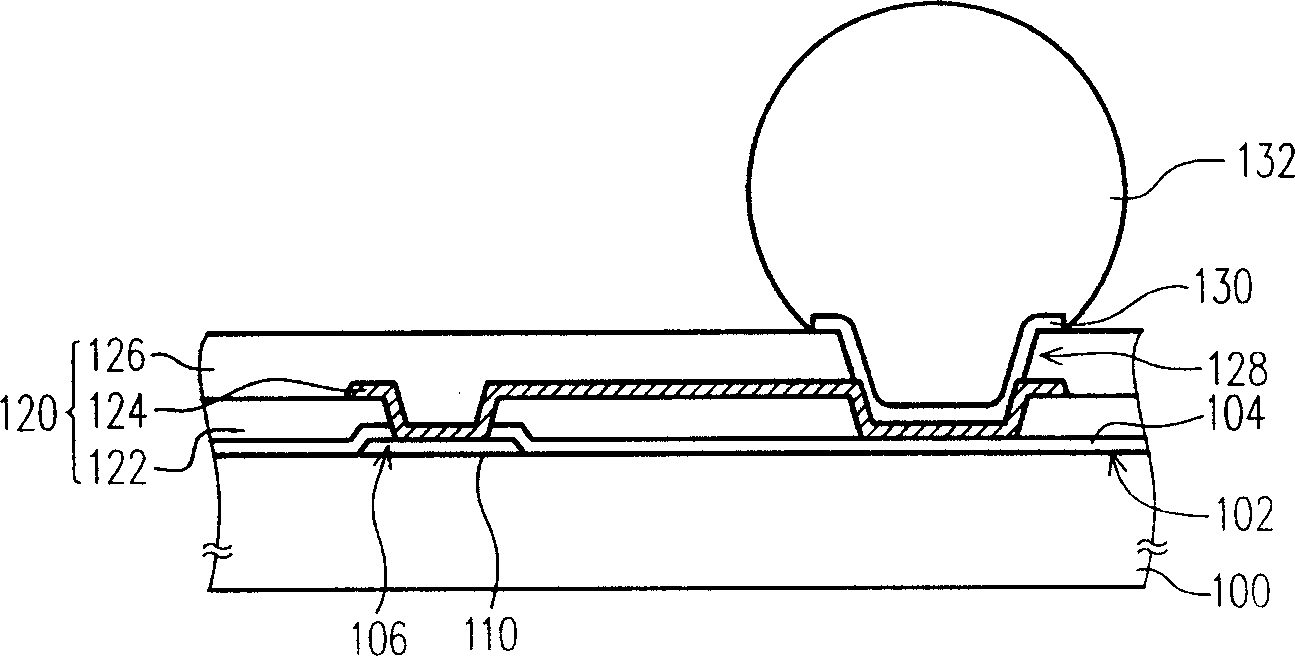
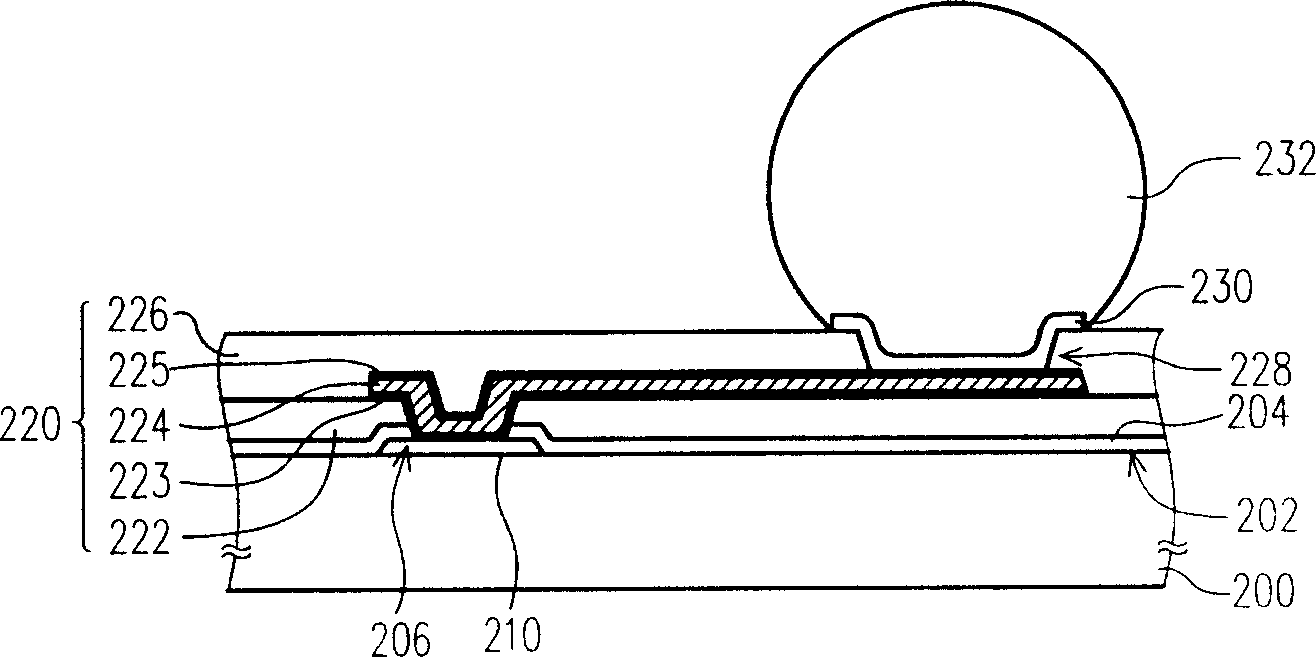
[0043] see figure 2 Shown is a schematic diagram of a redistribution layer according to a preferred embodiment of the present invention to define the lines and contact windows required for the subsequent bumping process. exist figure 2 Among them, there is a protective layer 204 on the active surface 202 of the wafer 200, and the protective layer 204 can be deposited from an organic protective material or an inorganic protective material, which covers the active surface 202 of the wafer 200, and the common protection Layer 204 , s...


PUM


Abstract

The invention is designed for use in a wafer to define a circuit and a contact window required by next bumping process. The re-wiring layer is located on a wafer's active side and has a line construction mainly comprising a first metal layer, a second metal layer and a conducting layer. Wherein, said conducting layer is mad of aluminum material, and said first and second metal layer are respectively overlapped on each of two side of said conducting layer. The connectivity between the first and second metal layers and a high polymer is higher than the one between said conducting layer and said high polymer. Said first and second metal layer can notably avoid the delaminating between a circuit layer and dielectric layer, and improve the reliability of wafer package.

Description

technical field [0001] The present invention relates to a multi-layer metal layer structure, in particular to an improved redistribution layer (Redistribution layer) and its circuit structure which improves the bonding reliability between the circuit layer and the dielectric layer. Background technique [0002] Flip Chip Interconnect Technology (FC for short) uses an area array to arrange multiple bonding pads on the active surface of a die, and Forming bumps on the bonding pads, and then flipping the chip, using these bumps to electrically and mechanically connect the bonding pads of the chip to the bonding pads (contacts) on the carrier, respectively, The chip can be electrically connected to the carrier through the bump, and electrically connected to the external electronic device through the circuit of the carrier. Since the flip-chip bonding technology (FC) is suitable for high-pin-count (High Pin Count) chip packaging structures, and has many advantages such as reduci...

Claims


Application Information

Patent Timeline
IPC IPC(8): H01L23/48H01L21/44H01L21/60H01L21/768H01L23/52
CPCH01L24/11H01L2224/11H01L2924/00012
Inventor 唐和明赵兴华王启宇樱桃
Owner ADVANCED SEMICON ENG INC
Why Eureka
Try Eureka