Multi-layer flexible printed circuit board, and method for fabricating it

a printed circuit board and flexible technology, applied in the direction of printed circuit manufacturing, printed circuit aspects, printed element electric connection formation, etc., can solve the problems of difficult etching of foils for micropatterning to give the intended circuit layer, the process of the method is long, and the micropatterning technology is limited to the increase in the density of fpc, so as to achieve good micropatterning of the circuit layer, high bonding reliability of the device, and good productivity

Inactive Publication Date: 2005-01-20
PANASONIC CORP
View PDF11 Cites 12 Cited by
  • Summary
  • Abstract
  • Description
  • Claims
  • Application Information

AI Technical Summary

Benefits of technology

[0017] Since such a composite comprising solder and different metal particles is used for the conductor for interlayer connection in the invention, the thermal expansion coefficient of the conductor may be optimized to realize high bonding reliability of the devices fabricated herein.
[0018] In the fabrication method of the invention, since the printed circuit layers are interconnected after they are formed, the process of the method does not have any influence on the circuit layers at all, and the method therefore enables good micropatterning of the circuit layers. In addition, since the interlayer connection is attained by an extremely simple process of filling each through-hole with a composite paste that comprises solder particles and different metal particles followed by fusing the solder particles, the method ensures good productivity.

Problems solved by technology

There is a limit of micropatterning technology to the increase in the circuit density of FPC.
However, the thick plating with copper shall increase not only the thickness of the copper plate film inside the through-holes but also the thickness of the copper foil to be a circuit layer, therefore making it difficult to etch the foil for micropatterning to give the intended circuit layer.
There are still other problems in that the process of the method is long and the productivity thereof is low.
In the method, however, the thermal expansion coefficient of solder is larger than that of the insulating layer, and when heated, the solder in the through-holes may expand more than the insulating layer and there may be a risk that the bonding interface between the circuit layer on the insulating layer and the solder may peel off.
To that effect, the soldering method is problematic in that the bonding reliability to heat of the devices fabricated therein is not good.
As mentioned above, the plated through-hole method in the related art for interlayer connection in multi-layer FPC is still problematic in point of the micropatterning of the circuit layers and of the productivity, though the bonding reliability of the devices fabricated therein is good.
On the other hand, the soldering method is also problematic in point of the bonding reliability of the devices fabricated thereon, though it solves the problems with the former method in point of the micropatterning of the circuit layers and of the productivity.

Method used


Image

  • Multi-layer flexible printed circuit board, and method for fabricating it
  • Multi-layer flexible printed circuit board, and method for fabricating it
  • Multi-layer flexible printed circuit board, and method for fabricating it

Examples


embodiment 1

[0049] (Embodiment 1)

[0050] Some embodiments of the multi-layer flexible printed circuit board of the invention are described below.

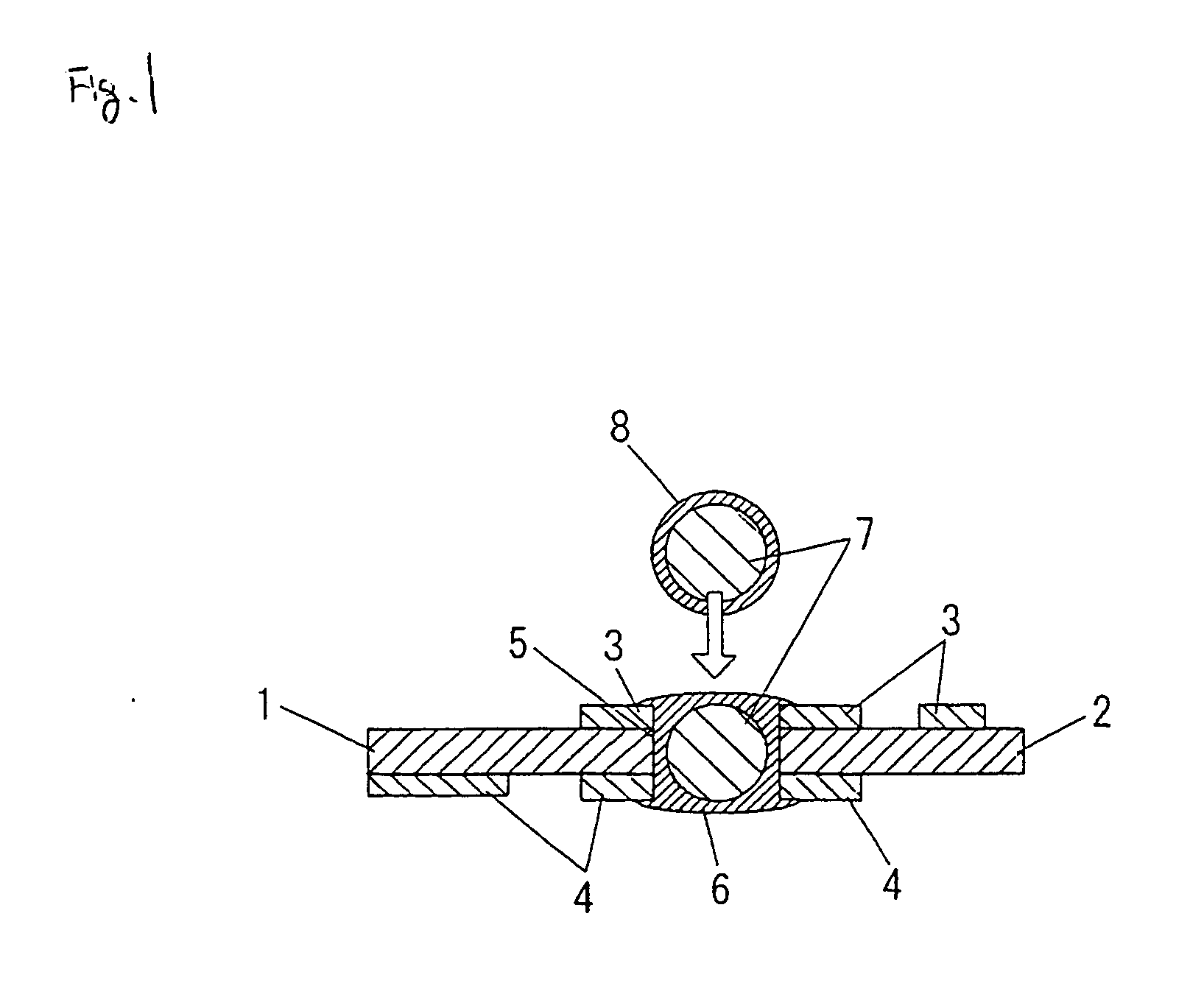
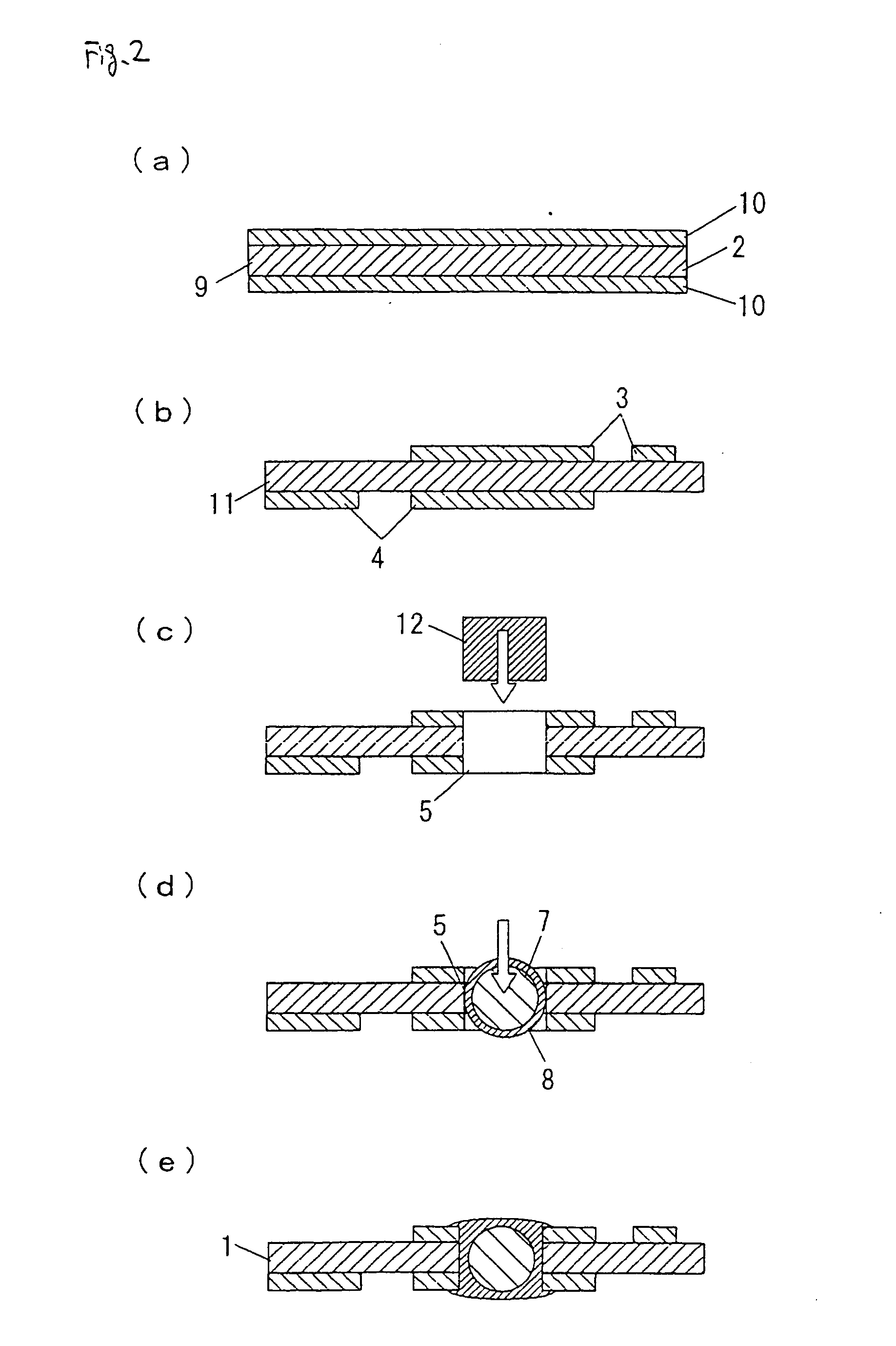
[0051]FIG. 1 is referred to for describing the multi-layer flexible printed circuit board of the invention. FIG. 1 is a cross-sectional view showing an essential part of one embodiment of the multi-layer flexible printed circuit board of the invention.

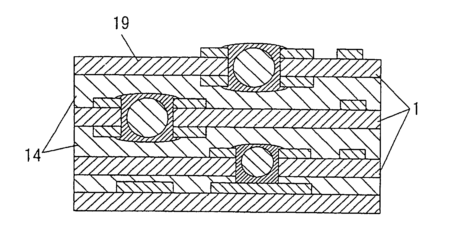
[0052] In FIG. 1, 1 is a multi-layer FPC having an upper circuit layer 3 and a lower circuit layer 4 formed on both faces of an insulating layer of a polyimide film, in which the circuit layers are interconnected to each other via a conductor 6 filled inside the through-hole 5. The conductor 6 is formed through fusing and solidification of a copper-core solder ball 8 that has a copper ball 7 inside it. The solder composition of the copper-core solder ball 8 may be any of eutectic solder, high-temperature solder, lead-free solder or the like, and any of these is favorable to the invention and may be used ...

embodiment 2

[0083] (Embodiment 2)

[0084] One embodiment of the multi-layer FPC of the invention is described below.

[0085]FIG. 5 is referred to for describing the multi-layer FPC of the invention. FIG. 5 is a cross-sectional view showing an essential part of one embodiment of the multi-layer FPC of the invention.

[0086] In FIG. 5, 101 is a multi-layer FPC having an upper circuit layer 103 and a lower circuit layer 104 formed on both faces of an insulating layer of a polyimide film, in which the circuit layers are interconnected to each other via a conductor 6 filled inside the through-hole 105. 107 is solder, and 108 is different metal particles. The different metal particles 108 are metal particles differing from the solder composition.

[0087] The conductor 106 contains different metal particles 108 inside the solder 107. The solder composition of the solder 107 may be any of eutectic solder, high-temperature solder, lead-free solder or the like, and any of these is favorable to the invention a...


PUM

PropertyMeasurementUnit
flexibleaaaaaaaaaa
thicknessaaaaaaaaaa
melting pointaaaaaaaaaa

Abstract

To provide an interlayer-connected, multi-layer flexible printed circuit board having high bonding reliability and most suitable for micropatterning the circuit layers in the device; and to provide a high-productivity method for fabricating the device. A multi-layer flexible printed circuit board, wherein a conductor is filled in the through-holes formed in the insulating layer in the direction of the thickness thereof so as to electrically interconnect the circuit layers formed on both faces of the insulating layer, and wherein the conductor contains inside it, a copper-core solder ball having a copper ball as a core thereof.

Description

BACKGROUND OF THE INVENTION [0001] 1. Field of the Invention [0002] The present invention relates to a flexible printed circuit board with various SMT (surface mount technology) chips mounted on the surface thereof, in particular, to such a multi-layer flexible printed circuit board of high bonding reliability and to a method for fabricating it. [0003] 2. Description of the Related Art [0004] The recent tendency in the art toward down-sized, lightweight and multi-function electronic appliances brings about further increase in the circuit density of the flexible printed circuit board (hereinafter this may be abbreviated to FPC) to be used in such appliances. There is a limit of micropatterning technology to the increase in the circuit density of FPC. Accordingly, multi-layer FPC is now specifically noticed, which comprises multiple circuit layers laminated and in which the multiple circuit layers are three-dimensionally interconnected through insulating layers that are interconnectab...

Claims


Application Information

Patent Timeline
Patent Type & Authority Applications(United States)
IPC IPC(8): H05K3/40H05K3/46
CPCH05K3/4038H05K3/4046H05K3/4614H05K3/4623H05K2201/0215Y10T29/49153H05K2201/096H05K2201/10234Y10T29/49126Y10T29/49149H05K2201/0305
Inventor YOSHINO, TOYOKAZUNAKASHIMA, KOUJI
Owner PANASONIC CORP
Why Eureka
Try Eureka