Bi-directional signal level shift circuit

a shift circuit and bi-directional signal technology, applied in the field of i2c interface technique, can solve the problems of inconvenient use of optical transceivers, and achieve the effect of less space and smaller siz

Inactive Publication Date: 2005-06-09
SAMSUNG ELECTRONICS CO LTD
View PDF6 Cites 14 Cited by
  • Summary
  • Abstract
  • Description
  • Claims
  • Application Information

AI Technical Summary

Benefits of technology

[0021] Therefore, the present invention, which has been made in part to solve the above-mentioned problems associated with level shifting circuits. The present invention provides a circuit for shifting a level between two bi-directional signals having a different voltage level that occupies significantly less space on a substrate than level shifting circuits known heretofore.
[0022] The present invention also provides a circuit for shifting a level between two bi-directional signals with different voltage levels in I2C interfaces in optical transceivers used in optical communication networks, wherein the present invention is adapted for being manufactured with smaller size than known heretofore.
[0023] The above and other aspects of the present invention can be accomplished by the provision of a bi-directional signal level shift circuit comprising: a first analog s

Problems solved by technology

As described above, although there has is a known circuit that provides a signal level shift using optical trans

Method used


Image

  • Bi-directional signal level shift circuit
  • Bi-directional signal level shift circuit
  • Bi-directional signal level shift circuit

Examples


Embodiment Construction

[0029] Now, preferred aspects of the present invention will be described in detail with reference to the annexed drawings. In the following description made in conjunction with preferred aspects of the present invention, a variety of specific elements such as constituent elements of various concrete circuits are shown. The description of such elements has been made only for a better understanding of the present invention. In other words, the elements are provided for purposes of illustration and not limitation, and those skilled in the art will appreciate that the present invention can be implemented without using the above-mentioned specific elements.

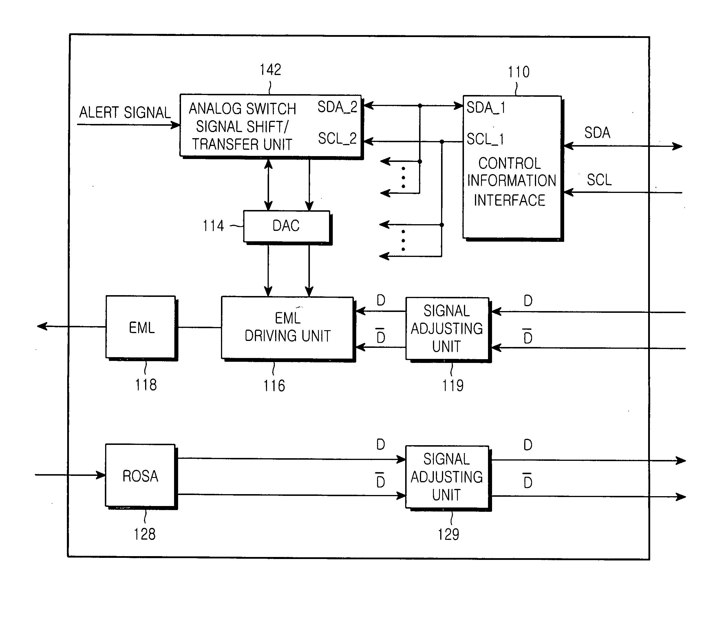
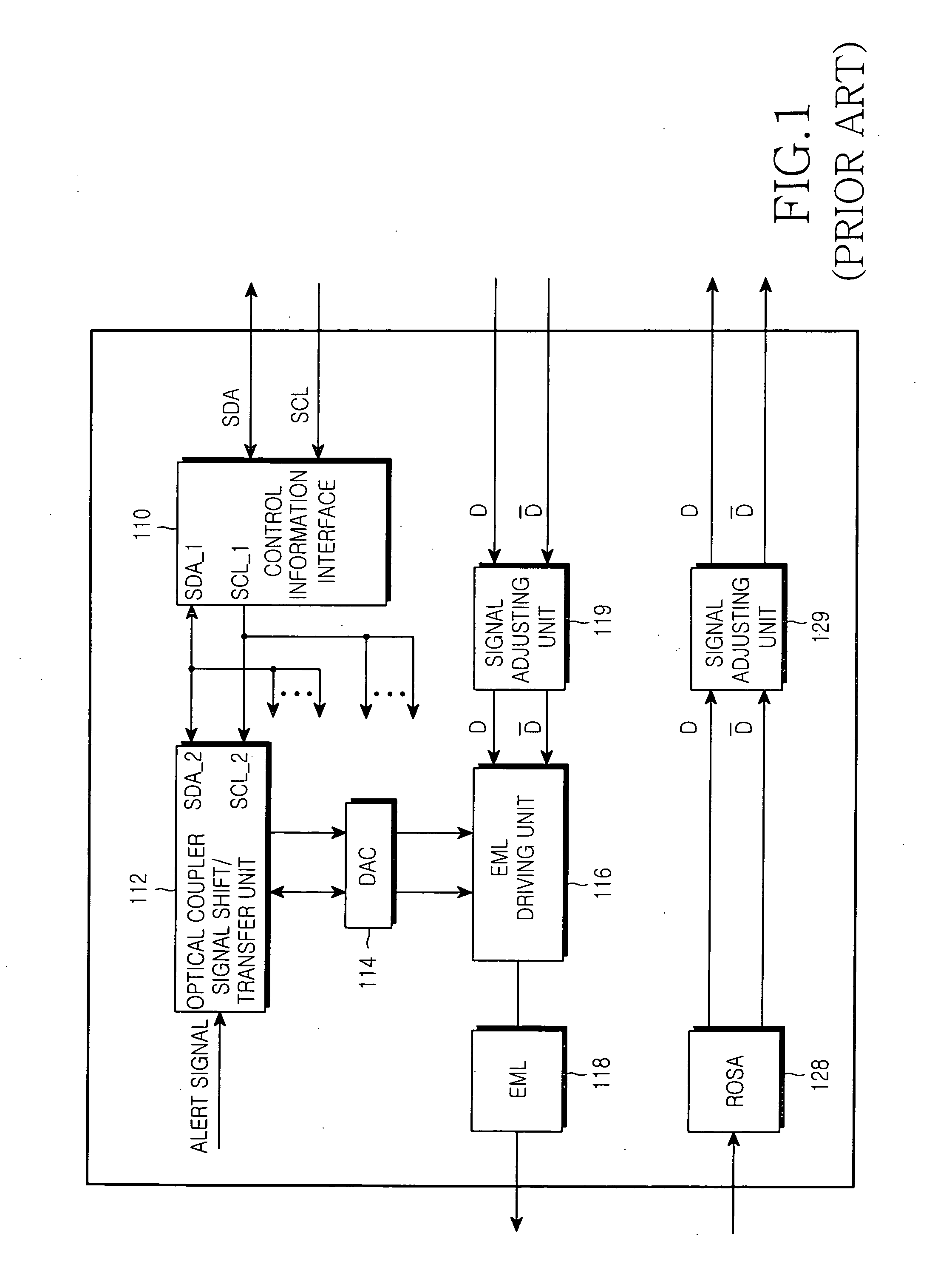
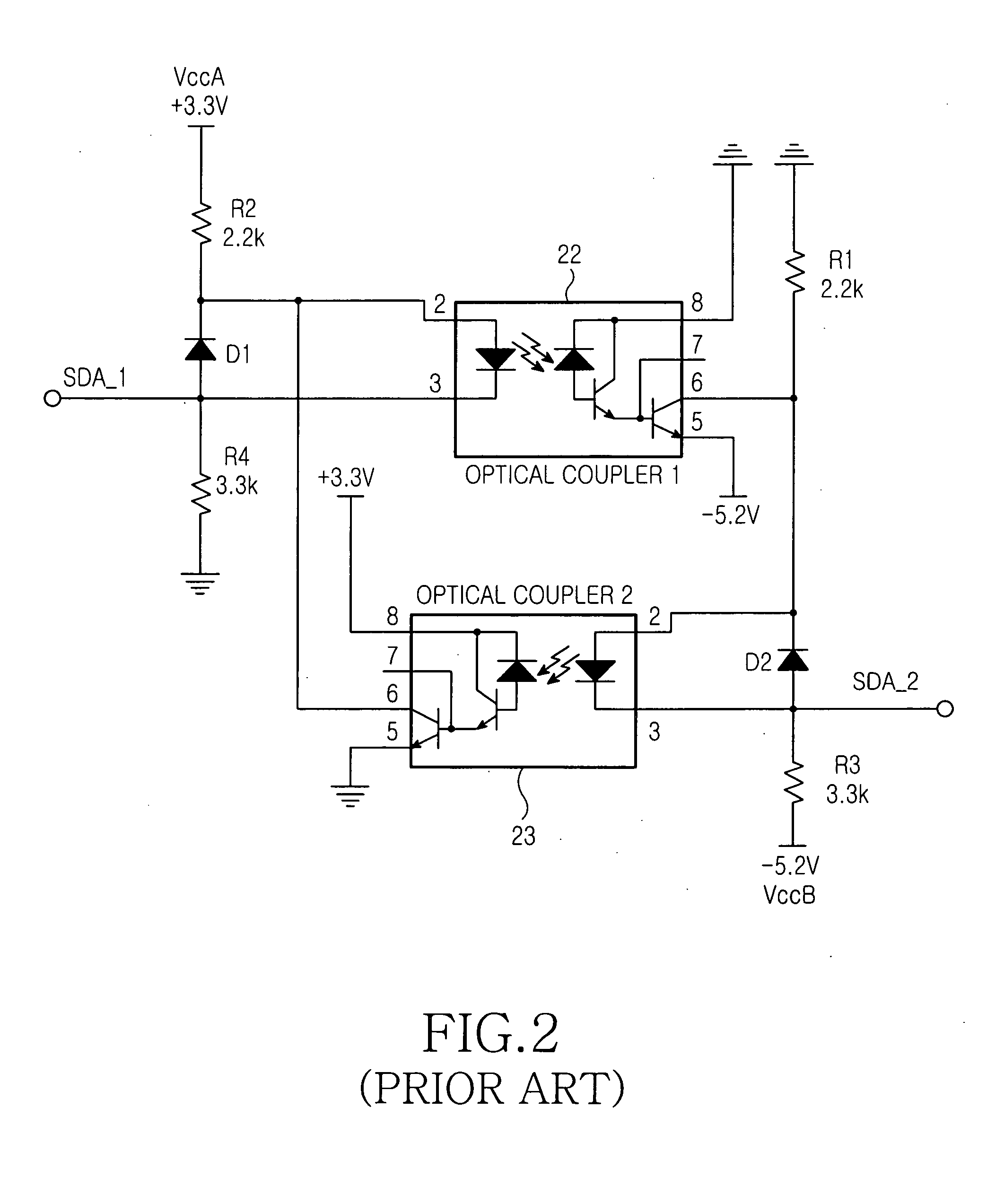
[0030]FIG. 4 is a schematic block diagram of an optical transceiver employing a bi-directional signal level shift circuit for an I2C interface in accordance with an aspect of the present invention. Referring to FIG. 4, the optical transceiver employing the bi-directional signal level shift circuit in accordance with the present invent...


PUM


Abstract

A circuit for shifting a level between two bidirectional signals having different voltage levels. The circuit includes a first analog switch including a first switching control terminal connected to first directional signal stage, a first input terminal connected to a first level of operating voltage, and a first output terminal connected to a second directional signal stage, for performing a switching operation for the first input terminal and the first output terminal based on a state of logic level of a signal from the second directional signal stage. The circuit also includes a second analog switch including a second switching control terminal connected to the first directional signal stage, a second input terminal connected to a second level of operating voltage, and a second output terminal connected to the first directional signal stage for performing a switching operation for the second input terminal and the second output terminal based on a state of a logic level of a signal from the first directional signal stage.

Description

CLAIM OF PRIORITY [0001] This application claims priority from an application entitled “BI-DIRECTIONAL SIGNAL LEVEL SHIFT CIRCUIT”, filed in the Korean Intellectual Property Office on Dec. 5, 2003 and assigned Serial No. 2003-87898, the contents of which are hereby incorporated by reference. BACKGROUND OF THE INVENTION [0002] 1. Field of the Invention [0003] The present invention relates to a circuit for shifting a level between two bi-directional signals having different voltage levels that are usable for such optical transceivers in optical communication networks. More particularly, the present invention relates to an I2C interface technique using such a circuit. [0004] 2. Description of the Related Art[0005] In recent days, there has been a sudden increase of Internet users, as well as a rapid expansion of optical communication networks for third generation mobile communication. This increase in usage has created a demand for a variety of optical communication modules to accommod...

Claims


Application Information

Patent Timeline
IPC IPC(8): H03K19/0175H04B10/02
CPCH03K19/01759H03K19/017536H04B10/40H04B10/00
Inventor LEE, YEON-JUNLEE, YONG-GU
Owner SAMSUNG ELECTRONICS CO LTD
Why Eureka
Try Eureka