

Nonvolatile semiconductor memory device
a semiconductor memory and non-volatile technology, applied in semiconductor devices, digital storage, instruments, etc., can solve the problems of interrupting data stored in memory elements, affecting and affecting the memory elements (at tmr or cmr layer), so as to improve the reliability of data retention characteristics and reduce the stress of voltage and current.
- Summary
- Abstract
- Description
- Claims
- Application Information
AI Technical Summary
Benefits of technology
Problems solved by technology
Method used
Image

Examples
first embodiment
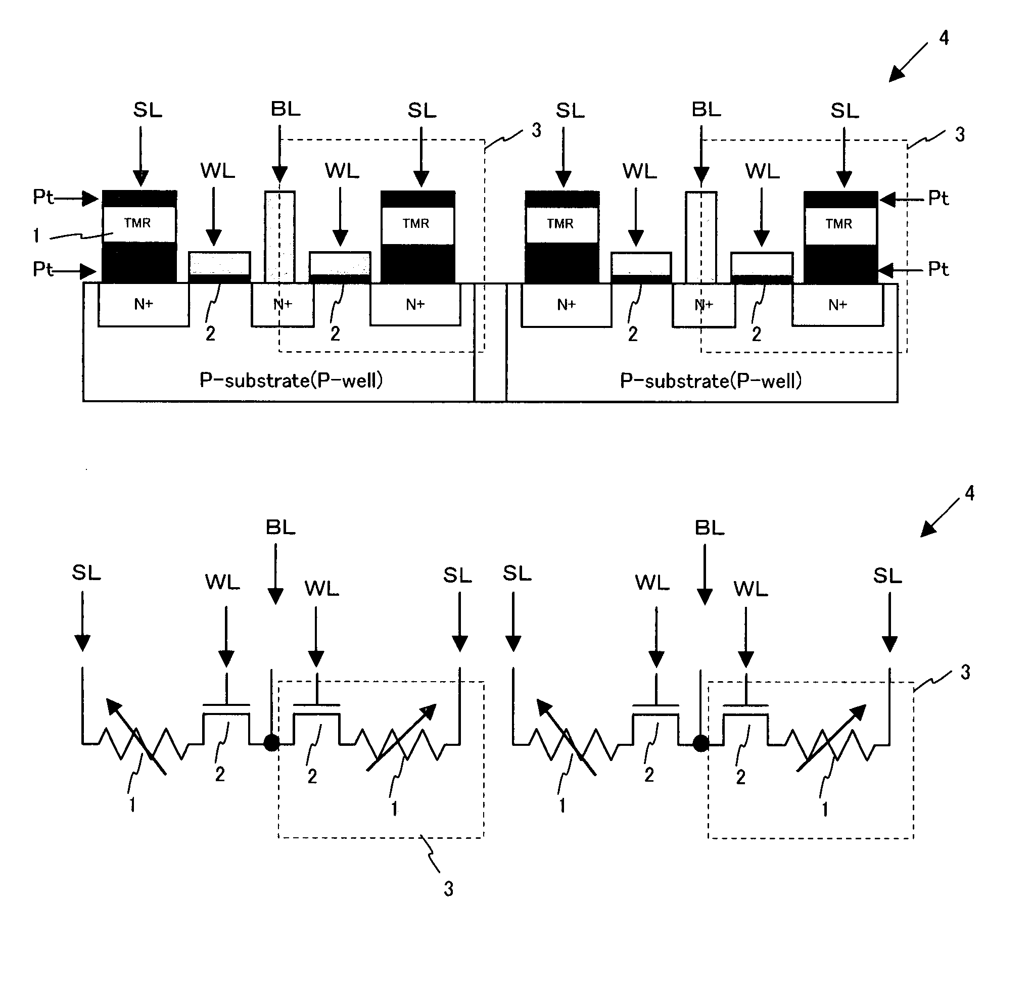
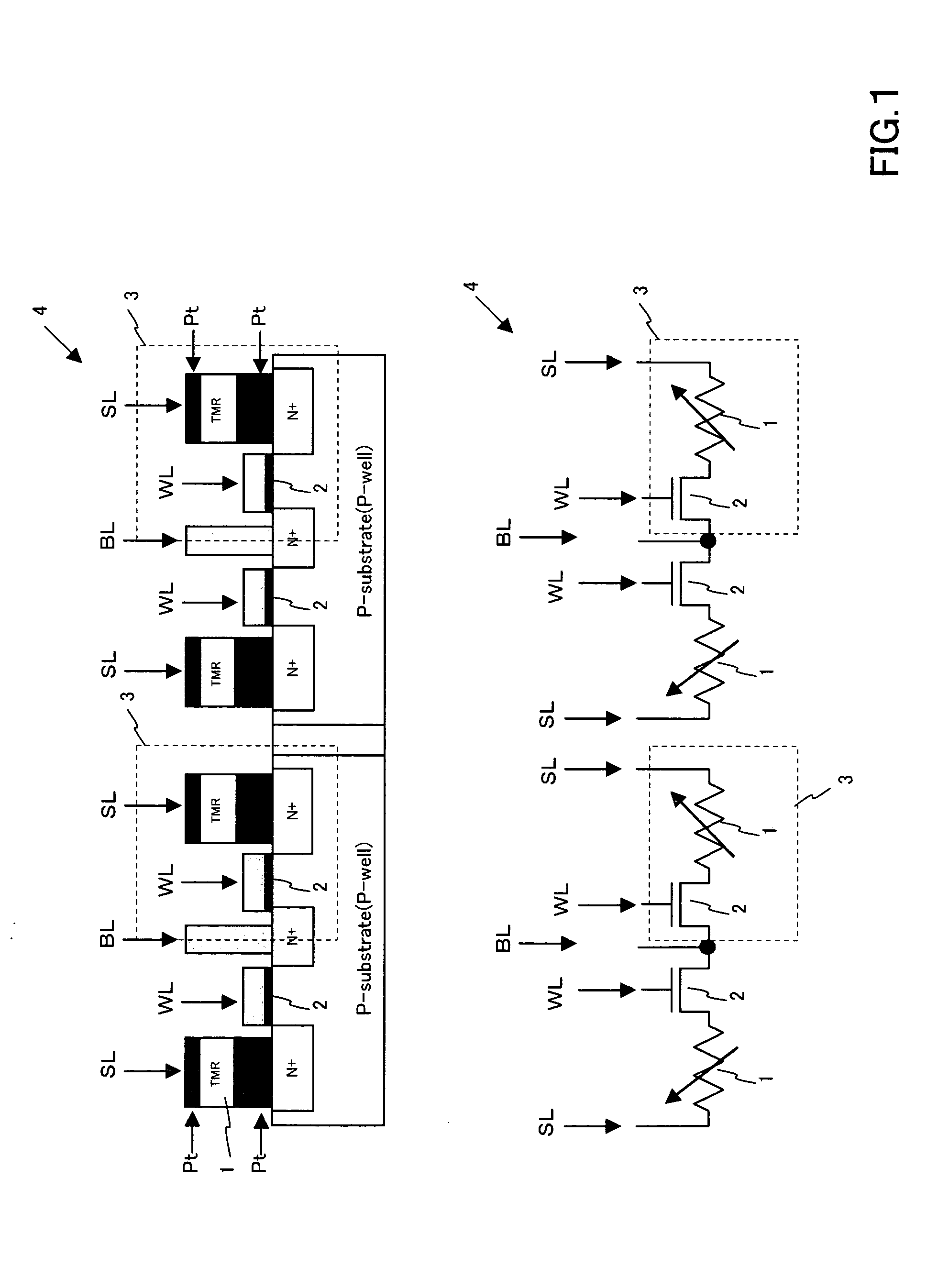
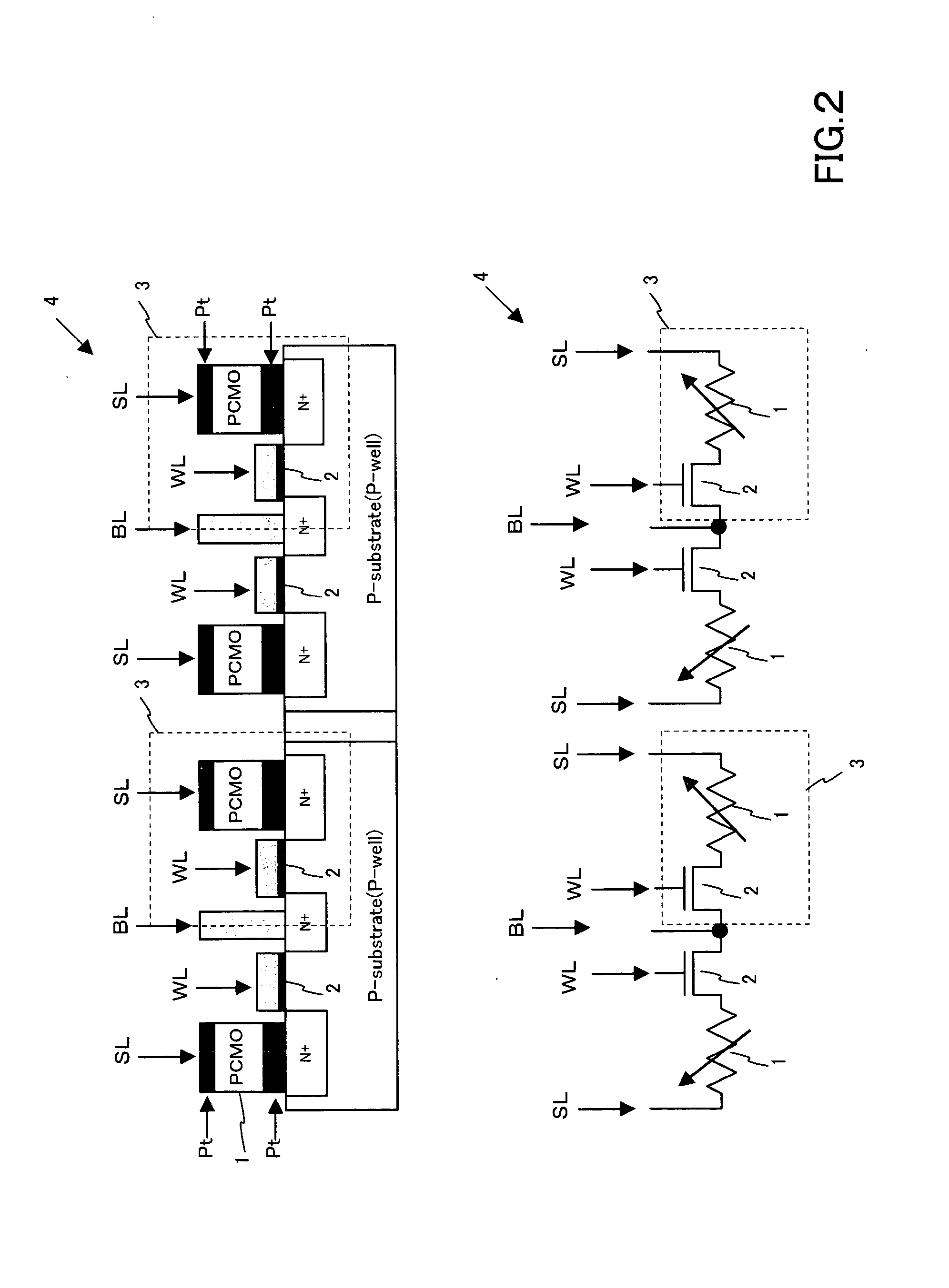
[0069]FIG. 1 illustrates a memory cell construction of the inventive device according to a first embodiment. A plurality of memory cells 3 are arranged in an array form of rows and columns to form a memory cell array 4 shown in FIG. 4. The inventive device in the first embodiment is provided in the form of an MRAM with the spin injection method. The memory cell 3 has a construction in that, as shown in FIG. 1, one end of a variable resistance element 1 including a TMR layer and a source of a selection transistor 2 are connected to each other to form a series circuit; a bit line BL is not directly connected to the variable resistance element 1, but is connected to a drain of the selection transistor 2; and a source line SL is connected to the other end of the variable resistance element 1. In the memory cell array, the bit line BL is commonly connected to the drains of the selection transistors 2 aligned along the column direction, the source line SL is commonly connected to the othe...
second embodiment
[0098] The second embodiment of the inventive device will be described. The primary construction is identical to that of the first embodiment but differentiated by the application of a pulsed voltage at the reset operation. FIG. 10 illustrates an application of voltage at the reset operation of the second embodiment. The second embodiment connects the selected source line SLs constantly with 5 V in place of the resetting pulsed input, the selected bit line BLs in a sub-sector of one byte (8 bits) with the ground potential GND, and the selected word line WLs with a pulsed voltage which has a pulse width of 1000 ns and shifts from 0 V to 7 V and then to 0 V in order to reset the memory cell 3 in the sub-sector of one byte. This is followed by connecting the selected bit line BLs in the succeeding sub-sector of one byte (8 bits) with the ground potential GND and the selected word line WLs with the pulsed voltage which has a pulse width of 1000 ns and shifts from 0 V to 7 V and then to ...
third embodiment
[0099] The third embodiment of the inventive device will now be described. The primary construction is identical to those of the first and second embodiments but differentiated by the location of the source line SL in the memory cell array 4. The memory cell array 4 in the first or second embodiment has the source line SL like the word line WL provided at each row. The third embodiment allows the source line SL to be shared by two adjacent rows as shown in FIGS. 11 and 12. FIG. 11 illustrates an application of voltage to each signal line at the reset operation of the third embodiment. FIG. 12 illustrates an application of voltage to each signal line at the write operation of the third embodiment. As the source line is shared by two adjacent rows, its cross section can be increased thus minimizing the electric resistance. Also, as the number of the sector decoders 7 is decreased, the circuit construction can be simplified thus minimizing the installation area to be required.
[0100] M...
PUM
 Abstract
Description
Claims
Application Information