Mask evaluating method, mask evaluating system, method of manufacturing mask and computer program product

Inactive Publication Date: 2005-06-16
KK TOSHIBA
View PDF3 Cites 11 Cited by
  • Summary
  • Abstract
  • Description
  • Claims
  • Application Information

AI Technical Summary

Benefits of technology

[0018] According to an aspect of the present invention, there is provided a method of manufacturing a mask including manufacturing a predetermined number of good photomask, comprising: evaluating the photomask using a method of manufacturing a mask described in any one of

Problems solved by technology

For this reason, it is difficult to highly secure a yield of the photomask including the foregoing micro-fabricated mask pattern.
For example, the efficiency of development and trial of device

Method used


Image

  • Mask evaluating method, mask evaluating system, method of manufacturing mask and computer program product
  • Mask evaluating method, mask evaluating system, method of manufacturing mask and computer program product
  • Mask evaluating method, mask evaluating system, method of manufacturing mask and computer program product

Examples


first embodiment

[0029] (First embodiment)

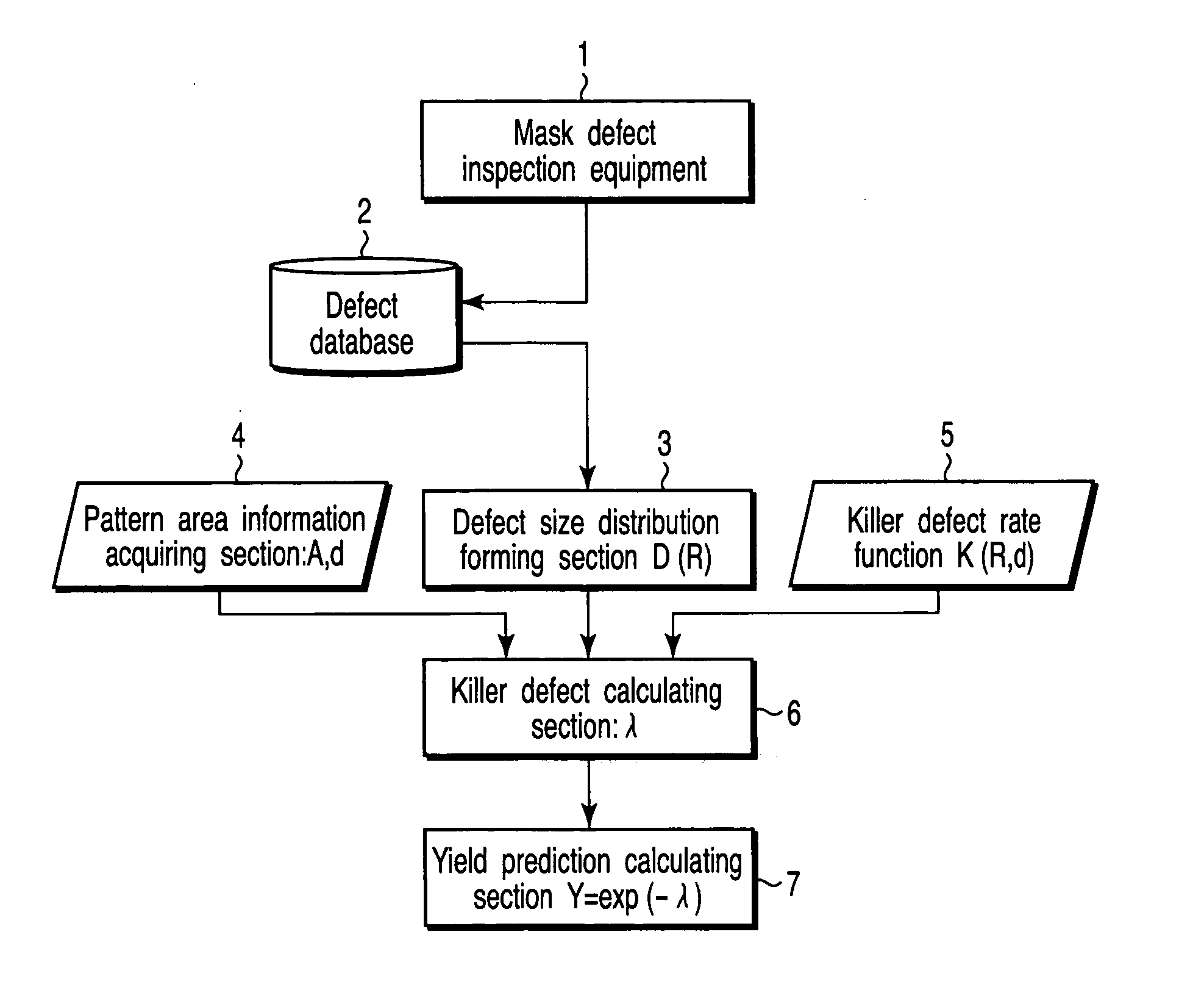
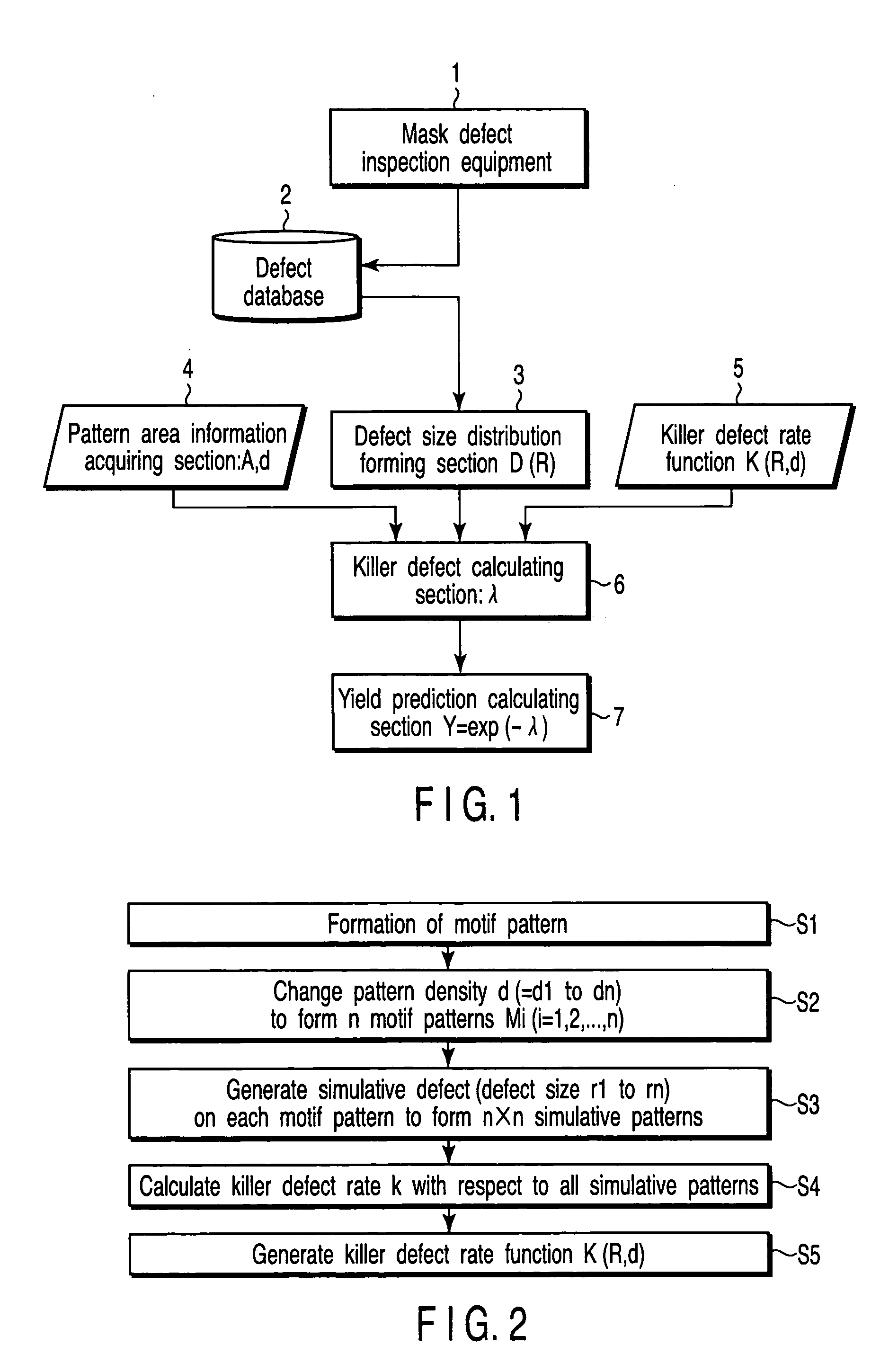
[0030]FIG. 1 is a block diagram showing a mask evaluation system according to the first embodiment of the present invention.

[0031] The mask evaluation system according to the present embodiment comprises:

[0032] a mask defect inspection equipment 1 which inspects defects on a photomask,

[0033] a defect database 2 which is stored with defect data relating to the photomask acquired by the mask defect inspection equipment 1,

[0034] a defect size distribution forming section 3 which forms a defect size distribution D(R) representing the number of defects per unit area on the photomask to a defect size R thereon based on the defect data stored in the defect database 2,

[0035] a pattern area information acquiring section 4 which acquires information including an area A of a main pattern area (region requiring predetermined defect accuracy (=region subjected to defect inspection) and a pattern density d in the foregoing main pattern area,

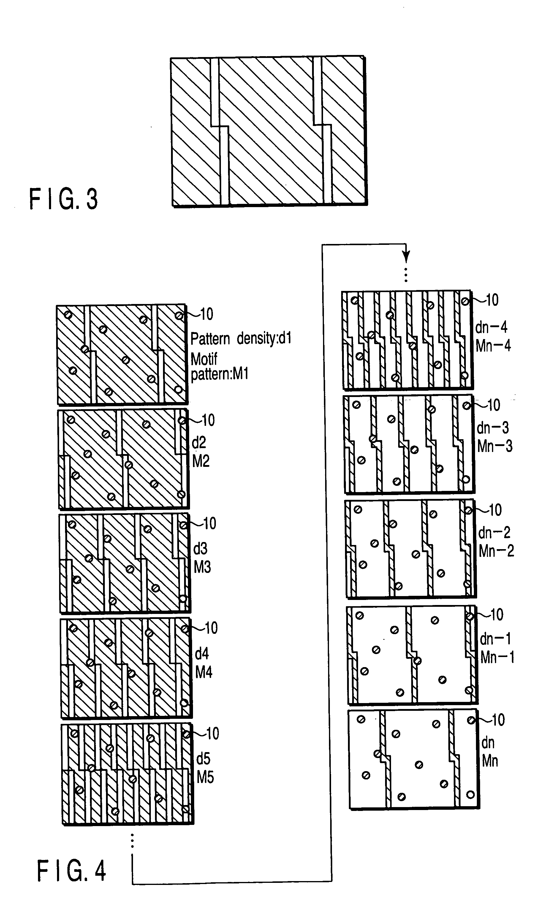
[0036] a killer defect ra...

second embodiment

[0076] (Second embodiment)

[0077] As described in the first embodiment, the predicted yield Y is given by the equation Y=epx(−λ), the number of killer defects λ is given by the equation λ=∫RA·K(R, d)·D(R) dR. Therefore, the predicted yield Y can be easily represented as a yield distribution expressed by a function using pattern area A and pattern density d as parameters. An example of yield map expressing the yield distribution is shown in FIG. 7.

[0078] The evaluation of the yield of the photomask using the yield map is carried out as follows.

[0079] The predicted yield Y is acquired every predetermined period. A yield map is generated from the acquired predicted yield Y every predetermined period. From these yield maps, s variable tendency in time of the whole yields is analyzed. Further, by paying attention to the pattern density d or pattern area A in a low yield range, the yield map of each period is compared and analyzed. An example of the analysis will be explained below.

[008...


PUM


Abstract

A photomask evaluating method comprises calculating a killer defect rate function with respect to a simulative defect pattern including a pattern of photomask and a plurality of defects, the killer defect rate function representing a killer defect rate of the simulative defect pattern with respect to a desired density of the pattern and a desired size of the plurality of defects, calculating the number of killer defects in an inspection region of the photomask based on an area of the photomask inspection region, a pattern density in the inspection region, the killer defect rate function and a defect size distribution representing the number of defects per unit area to a defect size range acquired from a photomask manufacturing step, and evaluating the photomask based on the calculated number of the killer defects.

Description

CROSS-REFERENCE TO RELATED APPLICATIONS [0001] This application is based upon and claims the benefit of priority from prior Japanese Patent Application No. 2003-372441, filed Oct. 31, 2003, the entire contents of which are incorporated herein by reference.BACKGROUND OF THE INVENTION [0002] 1. Field of the Invention [0003] The present invention relates to mask evaluating method, mask evaluating system, method of manufacturing mask and computer program product used in a lithography process. [0004] 2. Description of the Related Art [0005] As a pattern of semiconductor device is miniaturized, a patterns on the photomask (mask pattern), which is a master of a circuit pattern formed on a wafer is also miniaturize. The micro-fabricated mask pattern requires strict dimension accuracy and defect specifications. For this reason, it is difficult to highly secure a yield of the photomask including the foregoing micro-fabricated mask pattern. [0006] If the yield of the photomask is reduced, a ne...

Claims


Application Information

Patent Timeline
IPC IPC(8): G03C5/00G03F1/84G06F17/50H01L21/027
CPCG03F1/84
Inventor INOUE, MARI
Owner KK TOSHIBA
Why Eureka
Try Eureka