Programmable high speed I/O interface

a high-speed, interface technology, applied in the direction of logic circuit coupling/interface arrangement, pulse technique, instruments, etc., can solve the problems of slow circuits, slow device performance, and more complex electronic systems, and achieve the effect of comparatively simple high-speed input and output circuits

Inactive Publication Date: 2005-06-23
ALTERA CORP
View PDF4 Cites 14 Cited by
  • Summary
  • Abstract
  • Description
  • Claims
  • Application Information

AI Technical Summary

Benefits of technology

[0007] Accordingly, embodiments of the present invention provide methods and apparatus for providing either high-speed, or lower-speed inputs and outputs. An input and output structure having a high-speed input, a high-speed output, a low or moderate speed input, and an low or moderate speed output is provided. One of the input and output circuits are selected and the others are deselected. The high-speed input and output circuits are comparatively simple, in one example having only a clear signal for a control line input, and are able to interface to lower speed circuitry inside the core of an integrated circuit. The low or moderate speed input and output circuits are more flexible, for example, having preset, enable, and clear as control line inputs, and are able to support JTAG boundary testing. These parallel high and lower speed circuits are user selectable such that the input output structure is optimized between speed and functionality depending on the requirements of the application.

Problems solved by technology

Electronic systems are becoming more complex as they handle increasingly difficult tasks.
Unfortunately, increased flexibility results in slower circuits.
The same transistors that add functions and increase multiplexing insert parasitic capacitances and resistances, slowing device performance.

Method used


Image

  • Programmable high speed I/O interface
  • Programmable high speed I/O interface
  • Programmable high speed I/O interface

Examples


Embodiment Construction

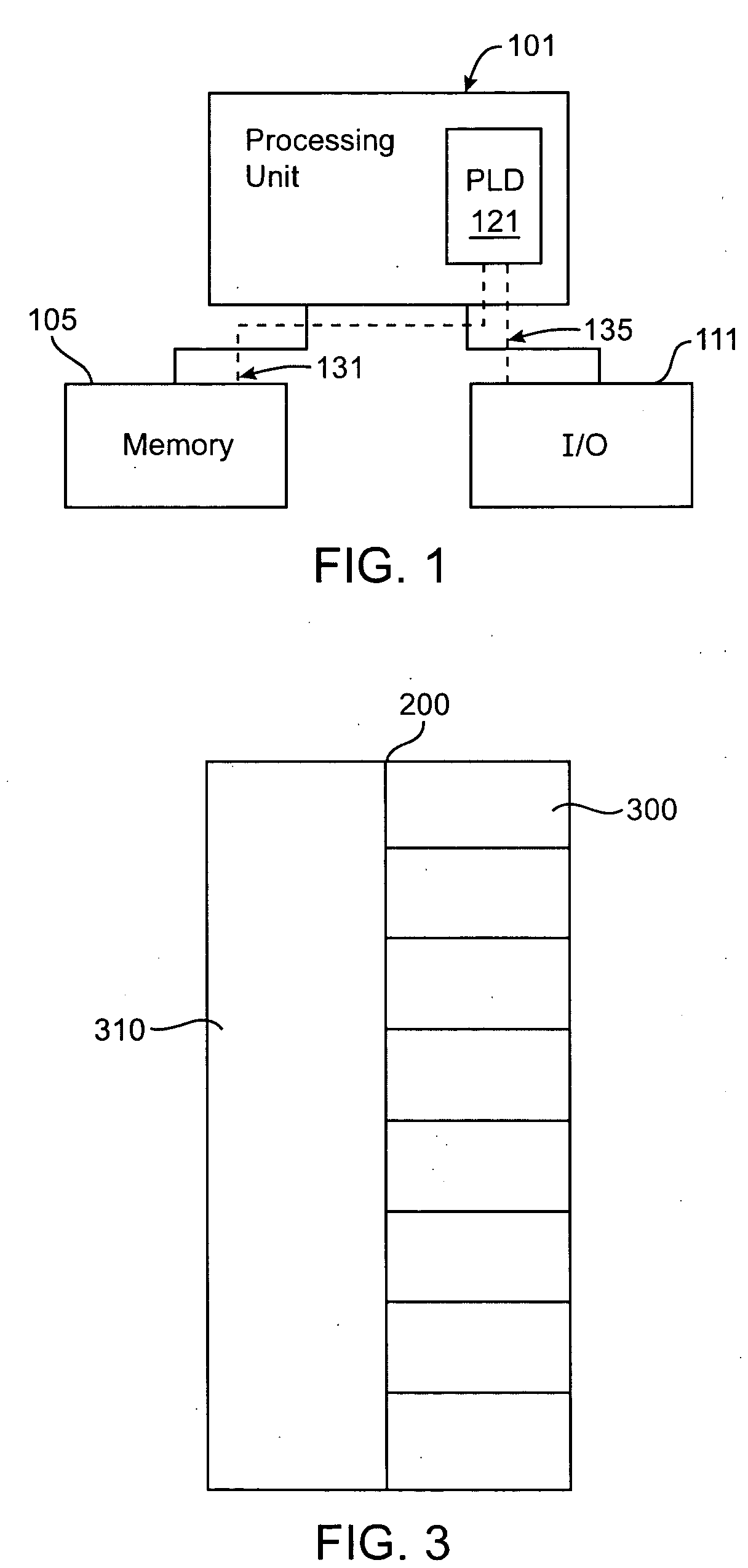
[0032]FIG. 1 shows a block diagram of a digital system, within which input and output interfaces consistent with the present invention may be embodied. The system may be provided on a single board, on multiple boards, or within multiple enclosures. Though embodiments of the present invention are useful in electronic and integrated circuits in general, they are particularly useful in programmable logic devices. FIG. 1 illustrates a system 101 in which such a programmable logic device 121 may be utilized. Programmable logic devices or programmable logic integrated circuits are sometimes referred to as a PALs, PLAs, FPLAs, PLDs, CPLDs, EPLDs, EEPLDs, LCAs, or FPGAs and are well-known integrated circuits that provide the advantages of fixed integrated circuits with the flexibility of custom integrated circuits. Such devices allow a user to electrically program standard, off-the-shelf logic elements to meet a user's specific needs. Examples of current programmable logic devices are repre...


PUM


Abstract

Methods and apparatus for providing either high-speed, or lower-speed, flexible inputs and outputs. An input and output structure having a high-speed input, a high-speed output, a low or moderate speed input, and an low or moderate speed output is provided. One of the input and output circuits are selected and the others are deselected. The high-speed input and output circuits are comparatively simple, in one example having only a clear signal for a control line input, and are able to interface to lower speed circuitry inside the core of an integrated circuit. The low or moderate speed input and output circuits are more flexible, for example, having preset, enable, and clear as control line inputs, and are able to support JTAG boundary testing. These parallel high and lower speed circuits are user selectable such that the input output structure is optimized between speed and functionality depending on the requirements of the application.

Description

CROSS-REFERENCES TO RELATED APPLICATIONS [0001] This application is a continuation of U.S. patent application Ser. No. 10 / 229,342 filed Aug. 26, 2002, which claims the benefit of provisional application 60 / 315,904 filed Aug. 29, 2001, which is incorporated by reference.BACKGROUND OF THE INVENTION [0002] The present invention relates to input and output interfaces for integrated circuits, and more particularly to high performance interfaces that have a high degree of flexibility and configurability. [0003] Electronic systems are becoming more complex as they handle increasingly difficult tasks. Accordingly, the amount of data transferred between integrated circuits in these systems continues to climb. At the same time, system designers want smaller, lower pin-count packages that consume less space on the system's printed circuit boards. Thus, very high data rates are desirable at integrated circuit input and output pins. [0004] But it is also desirable for the circuits that form the ...

Claims


Application Information

Patent Timeline
Patent Type & Authority Applications(United States)
IPC IPC(8): G06F3/00G06F13/38H03K19/0175H03K19/173H03K19/177
CPCH03K19/017581H03K19/17788H03K19/17744H03K19/0175H03K19/017509H03K19/1774
Inventor WANG, BONNIE I.SUNG, CHIAKANGHUANG, JOSEPHNGUYEN, KHAIPAN, PHILIP
Owner ALTERA CORP
Why Eureka
Try Eureka