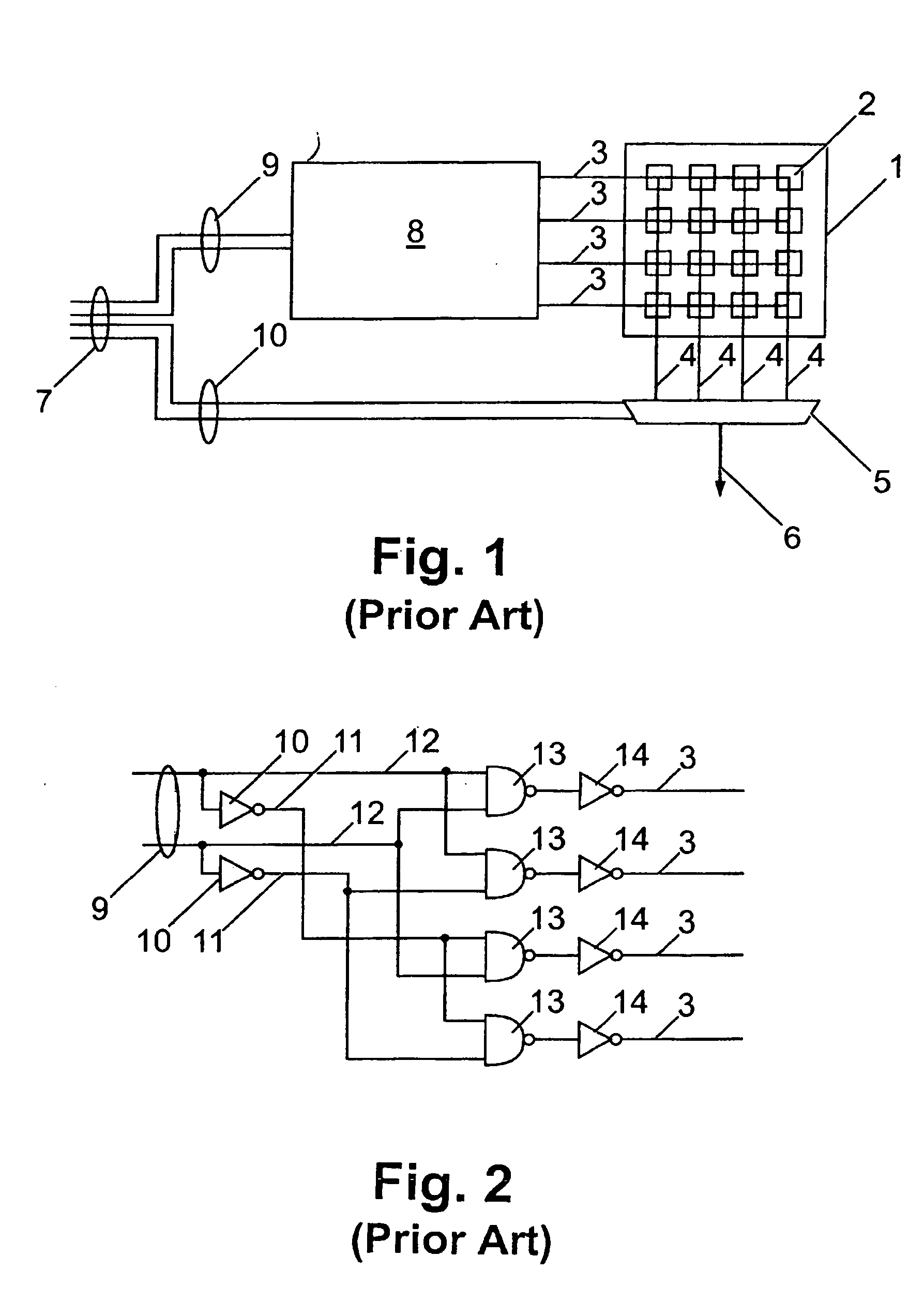
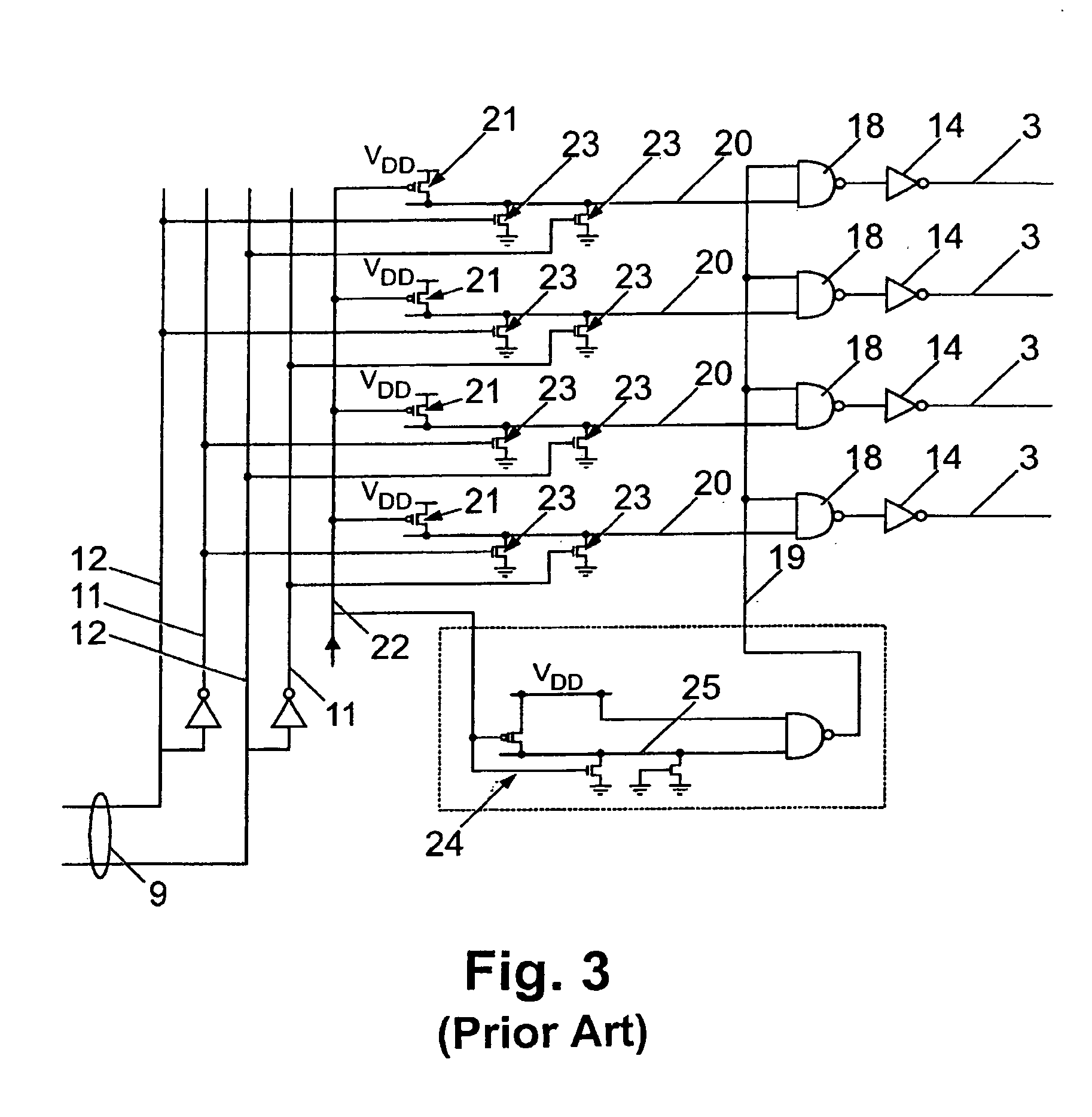
Decoder circuit

a decoder and circuit technology, applied in logic circuits, digital storage, instruments, etc., can solve the problems of large nand gate size, high current consumption, and large power consumption, and achieve the effect of reducing potential

Inactive Publication Date: 2005-06-30
AVAGO TECH INT SALES PTE LTD
View PDF4 Cites 14 Cited by
  • Summary
  • Abstract
  • Description
  • Claims
  • Application Information

AI Technical Summary

Benefits of technology

[0022] The first selection circuitry preferably comprises a selection transistor having its gate connected to the first decode node, its source connected to receive the first enable signal, and its drain arranged to provide a selection signal for the respective one of the output lines. There is suitably an inverter or other (e.g. non-inverting) drive means responsive to the selection signal to drive the respective one of the output lines. The first selection circuitry is suitably operable to select the respective one of the output lines by reducing the potential on the drain of the selection transistor, e.g. by drainage of that potential to the source of the selection transistor. There may be further precharge circuitry for precharging the gate of the selection transistor to a charging potential. The further precharge circuitry may comprise a further precharge transistor having its source connected to the precharge potential and its drain connected to the drain of the selection transistor. The said precharge transistor and the said further precharge transistor may be operable in response to a common precharge signal.

Problems solved by technology

This circuit is simple, but has a number of disadvantages if the number of address line inputs is increased.
However, the large NAND gates are relatively slow.
In almost all applications—and especially in battery-powered applications power consumption is very important.
However, in the system of FIG. 2 as the input lines 9 change values potentially many, or all, of the distributed address signals will change, giving rise to a high current consumption.
The current consumption is further increased by the need to generate an inverted version of each input line to the decoder.
However, the discharge of all the undesired decode lines gives rise to high power consumption, and the necessary delay before the timing enable signal is generated reduces the speed of operation of the circuit.

Method used


Image

  • Decoder circuit
  • Decoder circuit
  • Decoder circuit

Examples


Embodiment Construction

[0037] The circuits of FIGS. 4 to 6 take advantage of the fact that in a precharge structure of the type shown in FIG. 3 all but one of the decode lines discharges. Therefore, the discharge lines adjacent to the desired decode line (which does not discharge) will both discharge. In the circuits of FIGS. 4 to 6 the discharge of a decode line is used to derive a timing enable signal for another decode line.

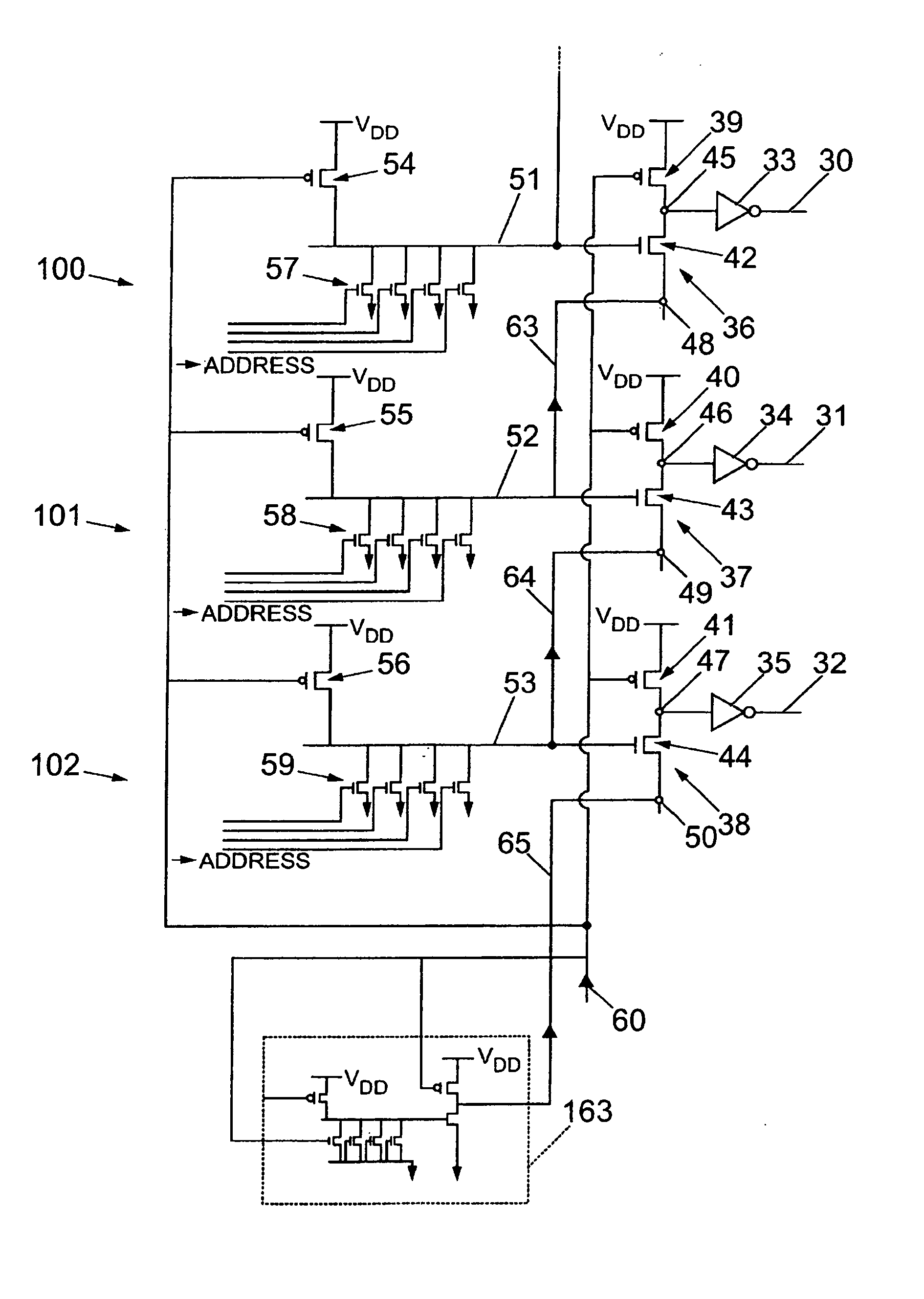
[0038] In the circuit of FIG. 4 three decode arrangements 100-102 are shown, each corresponding to a single wordline of an SRAM memory. (in a real circuit one decode arrangement would be provided for each wordline of the SRAM memory for which the decoder acted). Three of the wordlines of the SRAM memory are shown at 30-32. Each wordline is driven through a respective Inverter 33-35. The input to each inverter is generated by a respective gate arrangement 36-38 formed by two transistors 39-44. Each-gate arrangement comprises a first PMOS precharge transistor 39-41 connected with its...


PUM


Abstract

A decode circuit for selecting one of a plurality of output lines in dependence on the status of a plurality of input lines, the circuit comprising: a first decode arrangement comprising: a first decode node; first precharging circuitry for charging the first decode node to a charging potential; first discharging circuitry comprising a plurality of switching means each operable in dependence on the status of a respective one of the input lines to couple the first decode node to a discharging potential, and first selection circuitry coupled to a respective one of the output lines and operable in response to a first enable signal to select that output line if the first decode node has not discharged; and a second decode arrangement comprising: a second decode node; second precharging circuitry for charging the second decode node to a charging potential; second discharging circuitry comprising a plurality of switching means each operable in dependence on the status of a respective one of the input lines to couple the second decode node to a discharging potential; and second selection circuitry coupled to a respective one of the output lines and operable in response to a second enable signal to select that output line if the second discharge node has not discharged; wherein the first enable signal is derived from the potential of the second decode node.

Description

CROSS-REFERENCE TO RELATED APPLICATIONS [0001] This application is a continuation of U.S. patent application Ser. No. 10 / 232,255, titled, “Decoder Circuit,” filed on Aug. 29, 2002, (allowed), which is a continuation of U.S. patent application Ser. No. 09 / 759,832, titled, “Decoder Circuit,” filed Jan. 12, 2001 (U.S. Pat. No. 6,456,118), which claims priority to UK application 0000738.5, filed Jan. 13, 2000, all of which are incorporated herein by reference in their entireties.BACKGROUND OF THE INVENTION [0002] 1. Field of the Invention [0003] This invention relates to a decoder circuit, for example for use in memory addressing. [0004] 2. Background Art [0005]FIG. 1 shows an example of the structure of a static random access memory (SRAM) and its addressing circuitry. The memory 1 comprises a grid of memory cells 2 arranged in rows and columns. In this example there are four rows and four columns but typical SRAMs have many more rows and columns. All the cells in a row are connected t...

Claims


Application Information

Patent Timeline
Patent Type & Authority Applications(United States)
IPC IPC(8): G11C8/10G11C11/418
CPCG11C11/418G11C8/10
Inventor BEAT, ROBERT
Owner AVAGO TECH INT SALES PTE LTD
Why Eureka
Try Eureka