Modulator and semiconductor integrated circuit including modulator and wired or wireless communication device including modulator and semiconductor device
- Summary
- Abstract
- Description
- Claims
- Application Information
AI Technical Summary
Benefits of technology
Problems solved by technology
Method used
Image

Examples
first embodiment
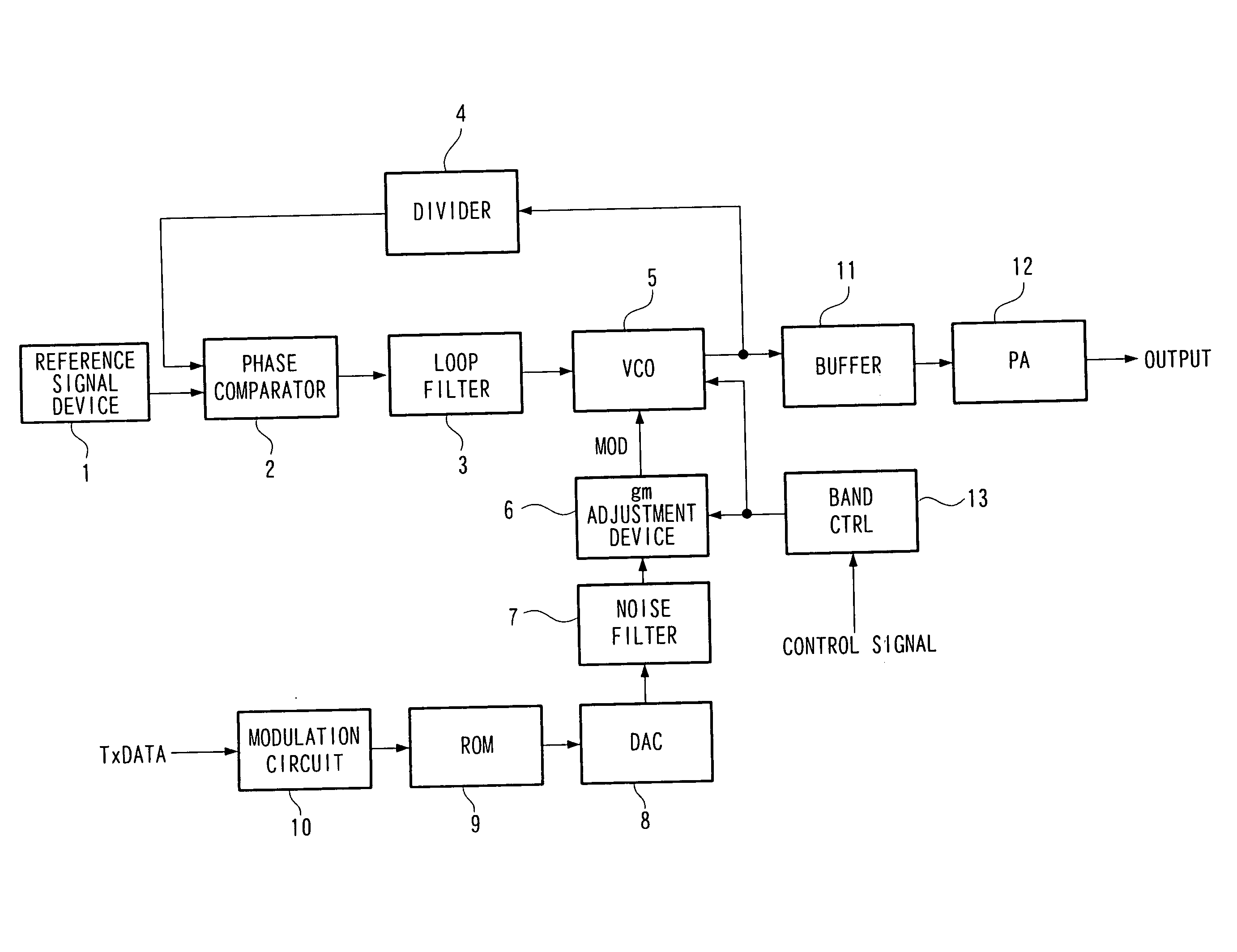
[0073]FIG. 1 is a block diagram showing the overall constitution of the modulator according to the first embodiment of the present invention. Further, constituent elements in each of the drawings below with substantially the same functions that correspond to the constituent elements described in FIG. 1 are shown with the same reference numerals assigned thereto.
[0074] In FIG. 1, 1 is a reference signal device, 2 is a phase comparator with two inputs that compares the phases of two inputted signals and outputs the phase difference as a signal, 3 is a loop filter that smoothes the output signal of the phase comparator, 4 is a divider, 5 is a VCO (Voltage Controlled Oscillator) that comprises a first input terminal to which a signal for controlling the emission frequency is inputted in order to constitute a PLL loop, a second input terminal to which a signal for controlling the frequency independently of the PLL loop is inputted, and a third input terminal to which a signal for switch...
second embodiment
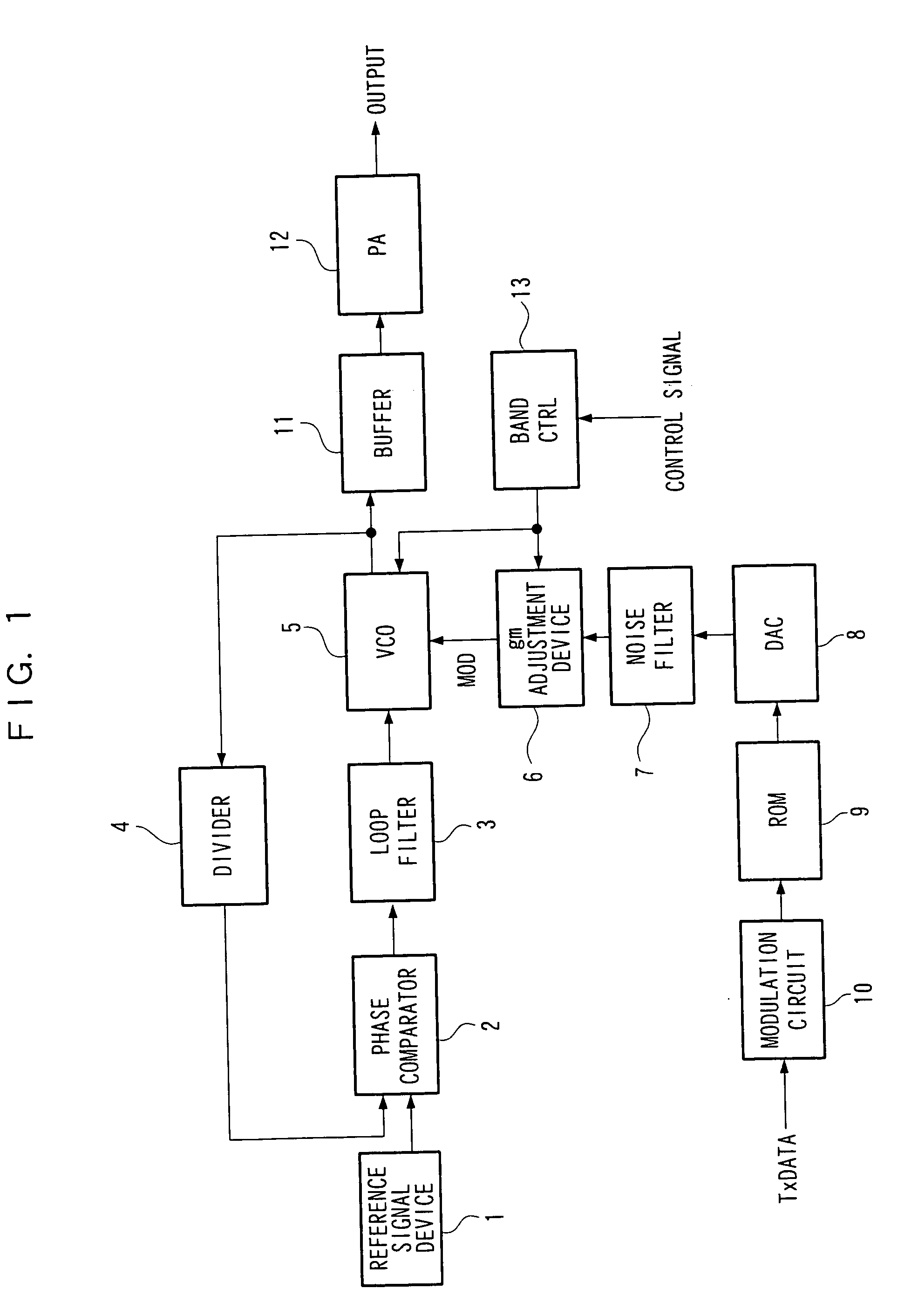
[0083]FIG. 4 is a block diagram showing the overall constitution of the modulator of the second embodiment of the present invention. As shown in FIG. 4, this modulator is constituted such that the output of the loop filter 3 in the block diagram shown in FIG. 1 is also inputted to the gm adjustment device 6.
[0084] When a variable capacitance diode is used to control the oscillation frequency of the VCO 5, any change in the oscillation frequency with respect to the frequency control voltage inputted to the VCO 5 is generally nonlinear. For example, when two points, which are points A and B marked with a round circle on curve BAND2 are taken by way of example as shown in FIG. 5, it can be clearly seen that the inclination at these points is different because curve BAND2 is not a straight line.
[0085] Further, the same is true of the other BAND. In the second embodiment with regard to curve BAND2, where line B is the modulation sensitivity with the required inclination, the output of ...
third embodiment
[0087]FIG. 7 is a block diagram showing the overall constitution of the modulator according to the third embodiment of the present invention. As shown in FIG. 7, this modulator is constituted such that the DAC 8 in the block diagram shown in FIG. 1 comprises a DC offset adjustment function for the output signal and a terminal for controlling this function, as well as a DAC CTRL 14 for adjusting the DC offset of the output signal of the DAC 8, wherein the control signal outputted by the DAC CTRL 14 is inputted to the offset control terminal with which the DAC 8 is provided.
[0088] When the DC level of the output signal of the gm adjustment device 6 varies as a result of fluctuations of the circuit characteristics in the process in which the output of the DAC 8 is inputted to the second input of the VCO 5 via the noise filter 7 and gm adjustment device 6, the center frequency of the output modulation signal of the VCO 5 also fluctuates. Further, because fluctuations of the oscillation...
PUM
 Abstract
Description
Claims
Application Information
 - R&D Engineer
- R&D Manager
- IP Professional
- Industry Leading Data Capabilities
- Powerful AI technology
- Patent DNA Extraction
Browse by: Latest US Patents, China's latest patents, Technical Efficacy Thesaurus, Application Domain, Technology Topic.
© 2024 PatSnap. All rights reserved.Legal|Privacy policy|Modern Slavery Act Transparency Statement|Sitemap