Image processing apparatus and control method thereof

a technology of image processing and control method, which is applied in the field of image processing apparatus, can solve the problems of circuit scale and cost increase of rearranging data, and circuit processing rate drop in the later stage, and achieve the effect of small circuit scale and high speed

Active Publication Date: 2020-04-02
CANON KK
View PDF0 Cites 0 Cited by
  • Summary
  • Abstract
  • Description
  • Claims
  • Application Information

AI Technical Summary

Benefits of technology

[0004]The present invention at least reduces the such problems with the past techniques, and provides an image processing apparatus, and a control method thereof, capable of rearranging data of a plurality of rows read out in parallel from an image sensor, at high speed and with a small circuit scale.

Problems solved by technology

As a result, as the number of rows to be read out in parallel increases, the circuit scale and cost for rearranging the data increases, the processing rate of the circuit in the later stage drops, and so on.

Method used


Image

  • Image processing apparatus and control method thereof
  • Image processing apparatus and control method thereof
  • Image processing apparatus and control method thereof

Examples


first embodiment

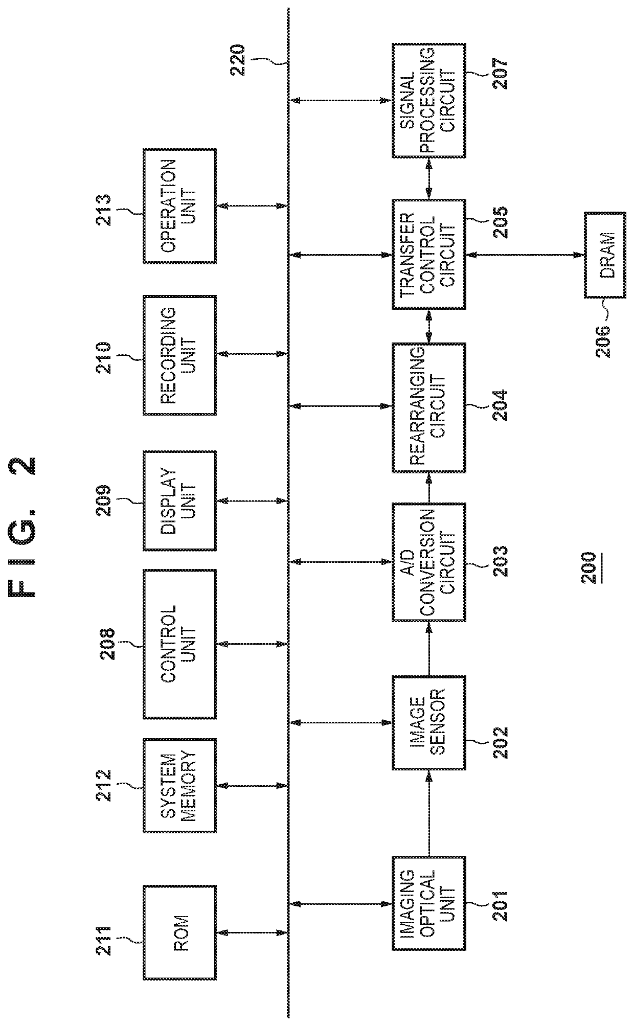
[0024]FIG. 2 is a block diagram illustrating an example of the functional configuration of a digital camera 200 serving as an example of an image processing apparatus according to a first embodiment of the present invention.

[0025]An imaging optical unit 201 includes a plurality of lenses including a focus lens, an aperture stop, and driving circuits for the lens, the aperture stop, and the like. The imaging optical unit 201 may or may not be removable from the digital camera 200.

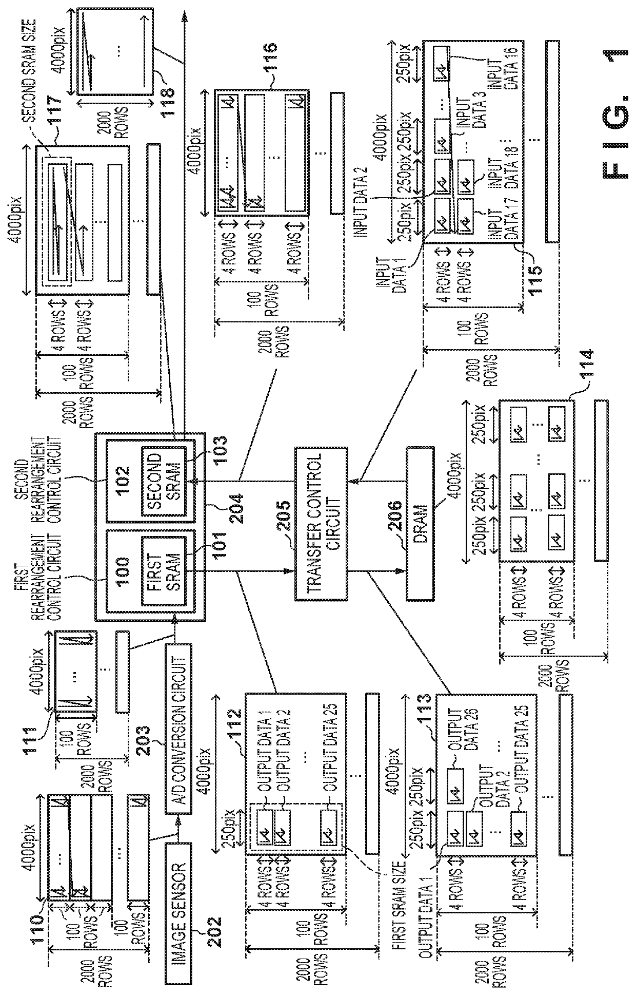
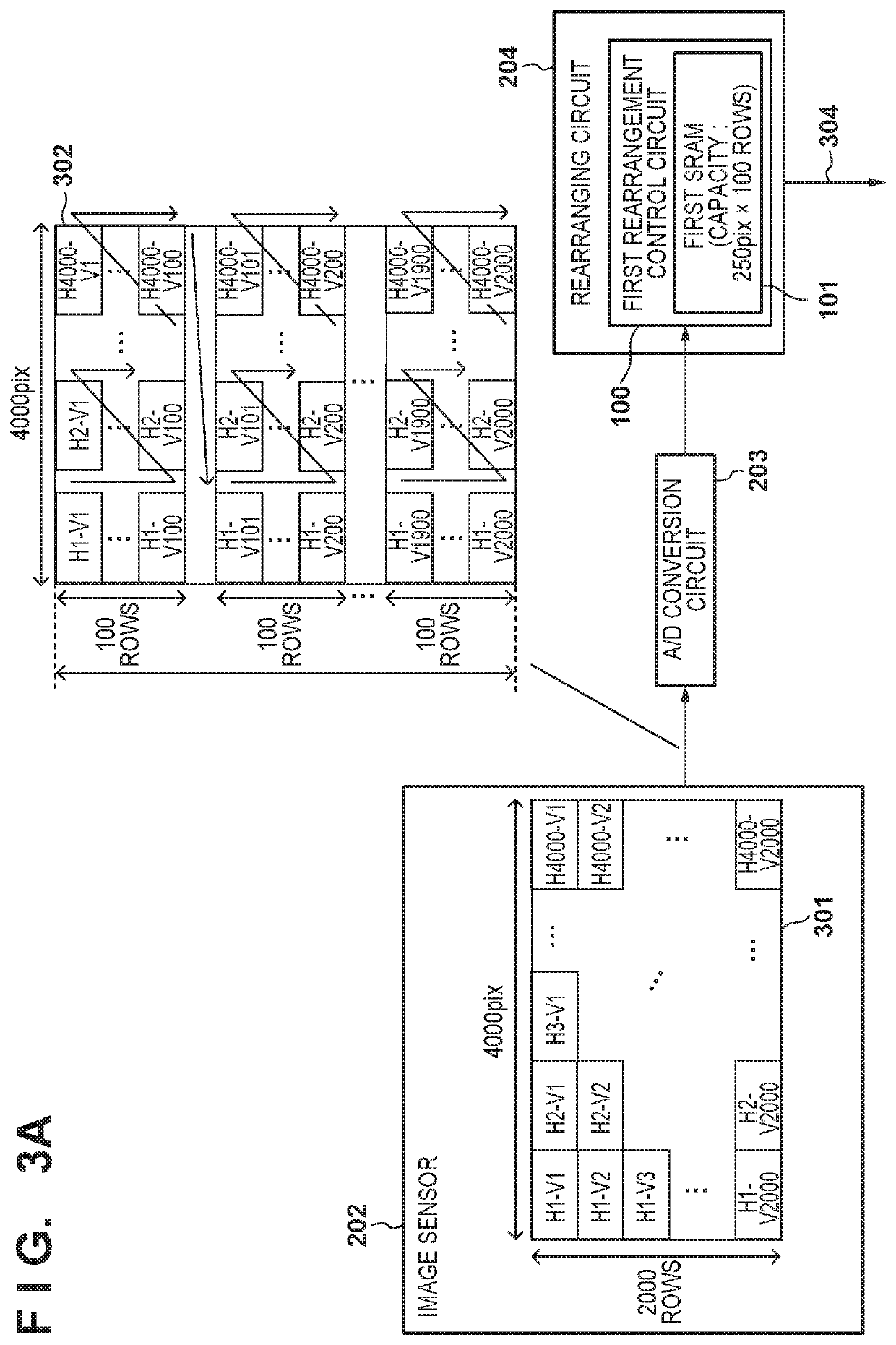
[0026]An image sensor 202 is a CMOS image sensor, for example, and includes a pixel array in which pixels, each including a photoelectric conversion unit, are arranged two-dimensionally, a horizontal scanning circuit and a vertical scanning circuit that supply control signals to the pixel array, and the like. The image sensor 202 has a mode in which signals are read out from the pixel array concurrently (in parallel) in units of a plurality of rows. In this mode, the data of one horizontally-arranged pixel (...

second embodiment

[0122]A second embodiment of the present invention will be described next. The present embodiment pertains to operations, carried out using the configuration described in the first embodiment, in which the number of rows read out from the image sensor 202 concurrently is not divisible by the number of rows in the first unit of rearrangement in the first SRAM (i.e., when m is not a multiple of o).

[0123]As an example, a case where 98 rows at a time are read out concurrently from the image sensor 202, and the first SRAM rearranges the data in units of four rows in the same manner as in the first embodiment (i.e., m=98 and o=4) will be described.

[0124]FIG. 10 is a diagram schematically illustrating the configuration according to the present embodiment, for rearranging 98 rows of data, which have been read out from the image sensor 202 concurrently, in the same order as if the data had been read out one row at a time. The configurations of the transfer control circuit 205 and the DRAM 20...

third embodiment

[0137]A third embodiment of the present invention will be described next. Like the second embodiment, the present embodiment pertains to operations, carried out using the configuration described in the first embodiment, in which the number of rows read out from the image sensor 202 concurrently is not divisible by the number of rows in the first unit of rearrangement in the first SRAM. The present embodiment differs from the second embodiment in that dummy pixels are not used.

[0138]To clarify the differences from the second embodiment, a case where 98 rows at a time are read out from the image sensor 202 concurrently, and the data is, like in the first embodiment, rearranged in units of four rows in the first SRAM, will be described as an example here.

[0139]FIG. 12 is a diagram schematically illustrating the configuration according to the present embodiment, for rearranging 98 rows of data, which have been read out from the image sensor 202 concurrently, in the same order as if the ...


PUM


Abstract

An apparatus takes data read out in parallel from m rows (2≤m<M) of a region, of an image sensor having M×N pixels, and stores n columns' worth (2≤n<N) of the read-out data in first memory. The apparatus stores the M×N pixels' worth of data in second memory by storing m×n pixels' worth of data in units of o×p pixels (2≤o<m, 2≤p≤n), and transfers the M×N pixels' worth of data, to third memory in the units of o×p pixels. The apparatus outputs the data stored in the third memory one row at a time so that the data are arranged in the original order.

Description

BACKGROUND OF THE INVENTIONField of the Invention[0001]The present invention relates to image processing apparatuses and control methods thereof.Description of the Related Art[0002]Various methods have been proposed with respect to accelerating data readout from image sensors. For example, a method is known in which data from a plurality of rows is read out in parallel. However, when a circuit in a later stage cannot process the data from a plurality of rows all at once, it is necessary to rearrange the data from the plurality of rows using a memory, in accordance with the unit by which the circuit in the later stage processes that data (Japanese Patent Laid-Open No. 2013-62714).[0003]According to Japanese Patent Laid-Open No. 2013-62714, Static Random Access Memory (SRAM) having a capacity equal to the number of rows to be read out in parallel is required in order to rearrange the data. As a result, as the number of rows to be read out in parallel increases, the circuit scale and c...

Claims


Application Information

Patent Timeline
Patent Type & Authority Applications(United States)
IPC IPC(8): H04N5/378H04N5/374
CPCH04N5/374H04N5/378G06T1/60H04N25/40H04N25/76H04N25/75H04N25/74H04N25/441
Inventor SUZUKI, SOICHIRO
Owner CANON KK
Why Eureka
Try Eureka