Pattern analysis method and pattern analysis apparatus

a pattern analysis and pattern technology, applied in the field of pattern analysis methods and pattern analysis apparatuses, can solve problems such as disadvantages that cannot be accurately calculated and unpractical

Inactive Publication Date: 2005-06-30
PANASONIC CORP
View PDF9 Cites 34 Cited by
  • Summary
  • Abstract
  • Description
  • Claims
  • Application Information

AI Technical Summary

Benefits of technology

[0063] In other words, the second pattern analysis apparatus is a pattern analysis apparatus for practicing the fifth or sixth pattern analysis method of the invention, and hence, the aforementioned effects can be attained.
[0064] As described so far, according to the present invention, the critical area, the number of single connection vias or the number of different-node near vias can be easily and accurately calculated. Therefore, when the critic

Problems solved by technology

However, in the case where the conventional critical area calculation method disclosed in, for example, Patent document 1 is applied to complicated interconnect patterns of LSIs with a recently increased degree of integration, it is necessary to calculate a critical

Method used


Image

  • Pattern analysis method and pattern analysis apparatus
  • Pattern analysis method and pattern analysis apparatus
  • Pattern analysis method and pattern analysis apparatus

Examples


embodiment 1

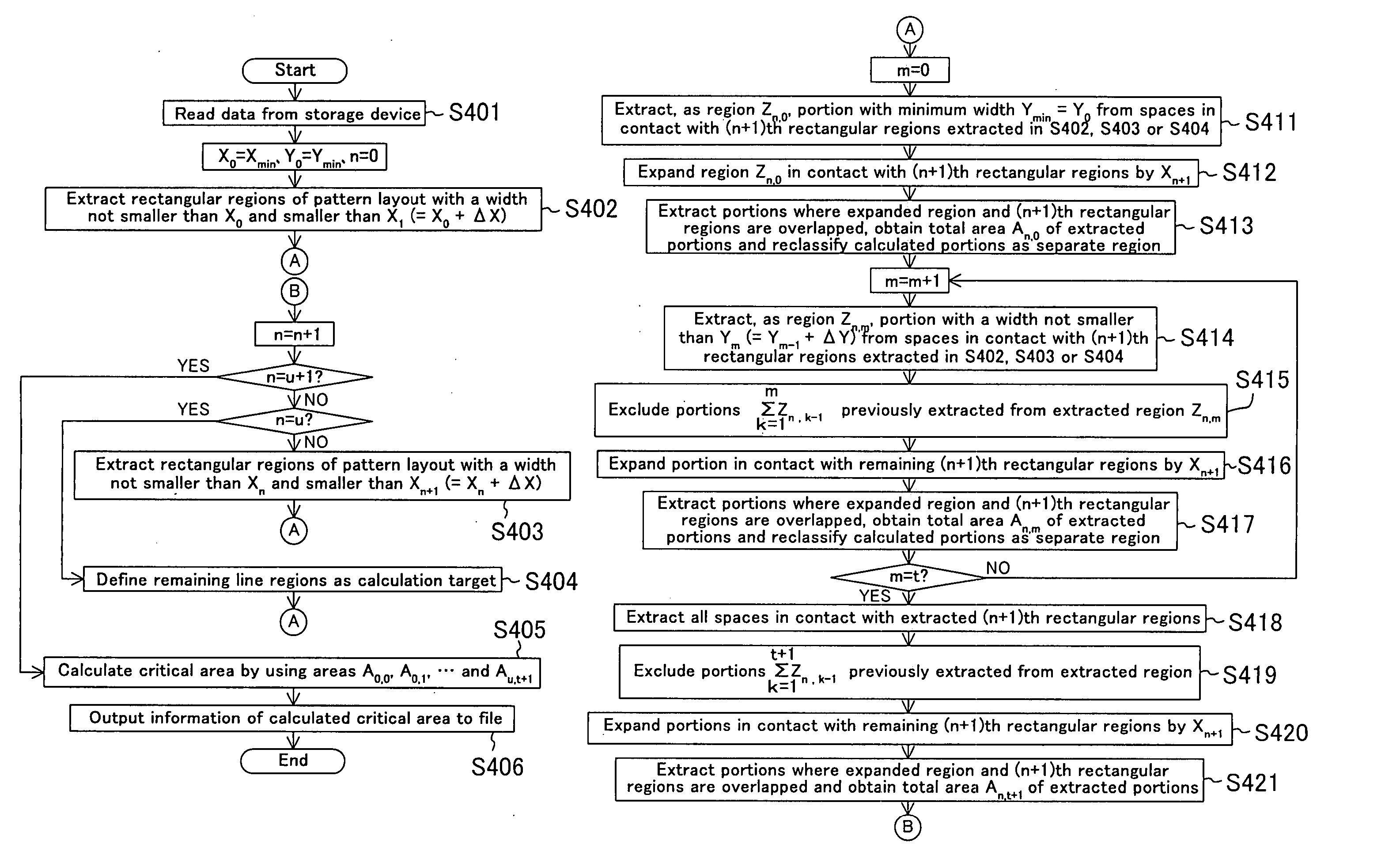
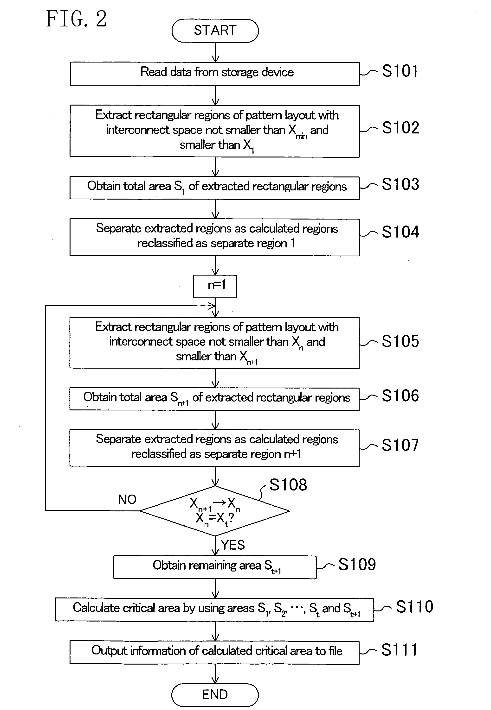
[0089] Now, a pattern analysis apparatus and a pattern analysis method according to Embodiment 1 of the invention will be described with reference to the accompanying drawings by exemplifying a case where a critical area of an interconnect pattern layout is calculated.

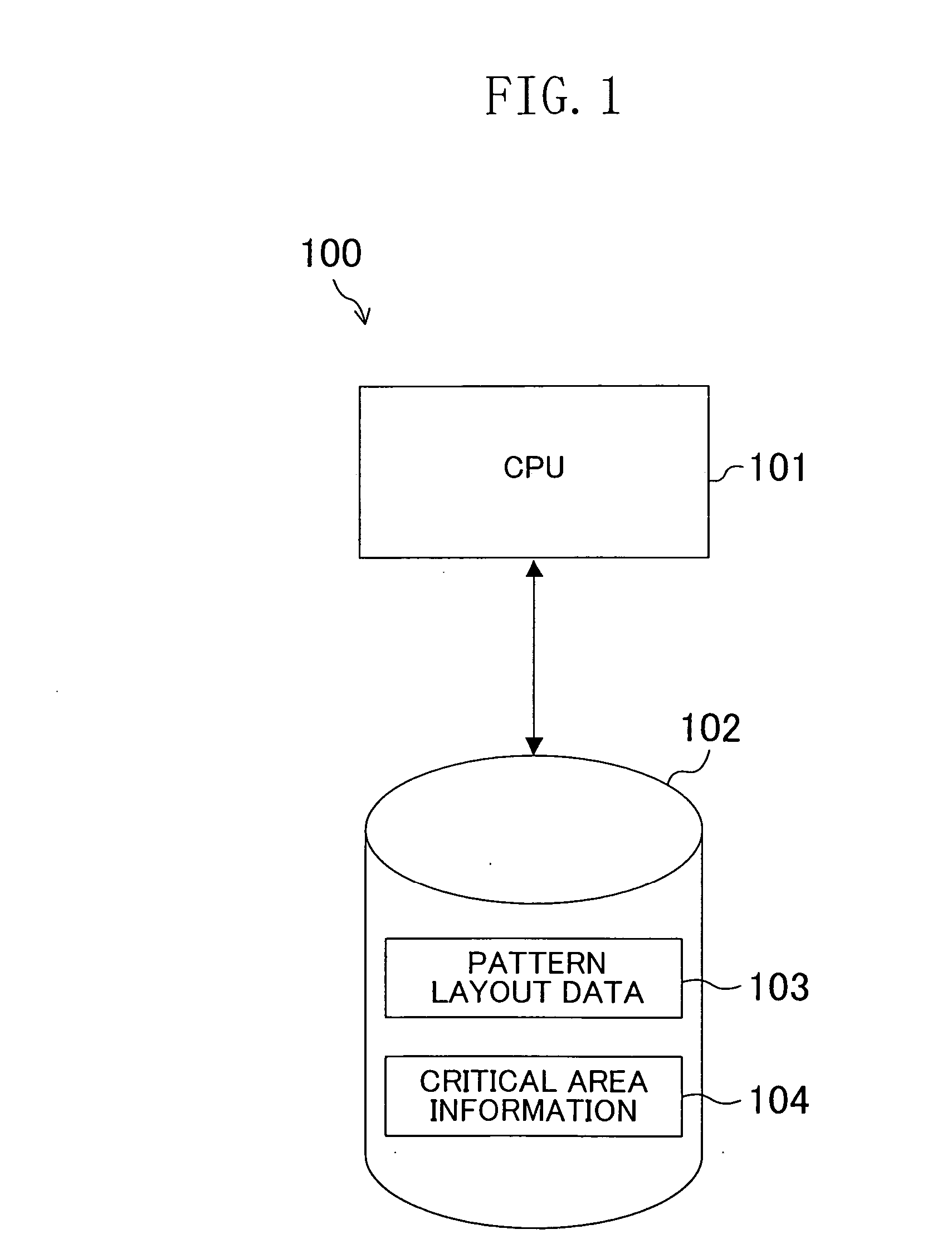
[0090]FIG. 1 is a diagram for showing an example of the architecture of the pattern analysis apparatus of Embodiment 1. As shown in FIG. 1, the pattern analysis apparatus 100 of this embodiment includes a central processing unit (CPU) 101 and a storage device 102 for storing pattern layout data 103 and critical area information 104. As operating means, the CPU 101 reads the pattern layout data 103 from the storage device 102 and executes the pattern analysis method of this embodiment described below by using the read pattern layout data 103. Also, as outputting means, the CPU 101 outputs, to the storage device 102, the critical area information 104 obtained as a result of the execution of the pattern analysis method o...

embodiment 2

[0112] Now, a pattern analysis apparatus and a pattern analysis method according to Embodiment 2 of the invention will be described with reference to the accompanying drawings by exemplifying a case where a critical area of an interconnect pattern layout is calculated.

[0113] An example of the architecture of the pattern analysis apparatus of Embodiment 2 is the same as that of Embodiment 1 shown in FIG. 1. Specifically, as shown in FIG. 1, the pattern analysis apparatus 100 of this embodiment includes a central control unit (CPU) 101 and a storage device 102 for storing pattern layout data 103 and critical area information 104. As operating means, the CPU 101 reads the pattern layout data 103 from the storage device 102 and executes the pattern analysis method of this embodiment described below by using the read pattern layout data 103. Also, as outputting means, the CPU 101 outputs, to the storage device 102, the critical area information 104 obtained as a result of executing the ...

embodiment 3

[0142] Now, a pattern analysis apparatus and a pattern analysis method according to Embodiment 3 of the invention will be described with reference to the accompanying drawings by exemplifying a case of calculating the number of single connection vias working as contacts for electrically connecting a lower interconnect and an upper interconnect in a multilayer interconnect structure of an LSI. It is noted that a yield YRV depending upon contact failure can be obtained by assigning the number of single connection vias obtained in this embodiment in, for example, Formula 6 (described in “Background of the Invention”) as the number N of vias.

[0143] First, a “single connection via” and “contact failure” will be described. FIGS. 7A and 7B are diagrams for explaining the “single connection via” and the “contact failure” in the cross-sectional structure of a part (multilayered interconnects) of a device. FIG. 7A shows electric connection between a lower interconnect and an upper interconne...


PUM


Abstract

A pattern analysis method includes: a first step of preparing pattern layout data including a plurality of first regions and a plurality of second regions; a second step of selecting either said plurality of first regions or said plurality of second regions as a target region in which a critical area of said pattern layout data is to be calculated; and a third step of extracting, from said target region, rectangular regions each having a width within a given range. The method further includes; a fourth step of obtaining a total area of said rectangular regions; and a fifth step of calculating said critical area by using said total area.

Description

CROSS-REFERENCE TO RELATED APPLICATIONS [0001] This application claims priority under 35 U.S.C. §119 on patent application No. 2003-395242 filed in Japan on Nov. 26, 2003 and No. 2004-139726 filed in Japan on May 10, 2004, the entire contents of which are hereby incorporated by reference.BACKGROUND OF THE INVENTION [0002] The present invention relates to a pattern analysis method and a pattern analysis apparatus employed for obtaining a yield of patterns, and more particularly, it relates to a pattern analysis method and a pattern analysis apparatus employed in fabrication of electronic devices such as semiconductor devices. [0003] In the fabrication of semiconductor devices such as LSIs, the cost of the semiconductor devices can be lowered by obtaining a large number of good LSIs from one semiconductor substrate (semiconductor wafer), namely, by improving the yield. The known factors for lowering the yield are, for example, defects such as particles causing a short-circuit or open ...

Claims


Application Information

Patent Timeline
IPC IPC(8): G06K9/00G06K9/46G06F17/50H01L21/82H01L27/02
CPCH01L27/0203G06F17/5081G06F30/398
Inventor TOHYAMA, YOKOITO, MITSUMI
Owner PANASONIC CORP
Why Eureka
Try Eureka