Semiconductor device and manufacturing method for the same

a semiconductor and manufacturing method technology, applied in mechanical equipment, refrigeration components, light and heating equipment, etc., can solve the problems of increasing manufacturing costs, affecting production efficiency, and difficulty in stacking general semiconductor devices on each other

Active Publication Date: 2005-07-14
KIOXIA CORP
View PDF2 Cites 86 Cited by
  • Summary
  • Abstract
  • Description
  • Claims
  • Application Information

AI Technical Summary

Problems solved by technology

Therefore, it is difficult to stack the general semiconductor devices on each other as they are.
For example, when a special semiconductor device is manufactured as the upper semiconductor device in order to remove the restrictions on the combination of the semiconductor devices, a rise of manufacturing cost or a drop of production efficiency is caused.

Method used


Image

  • Semiconductor device and manufacturing method for the same
  • Semiconductor device and manufacturing method for the same
  • Semiconductor device and manufacturing method for the same

Examples


first embodiment

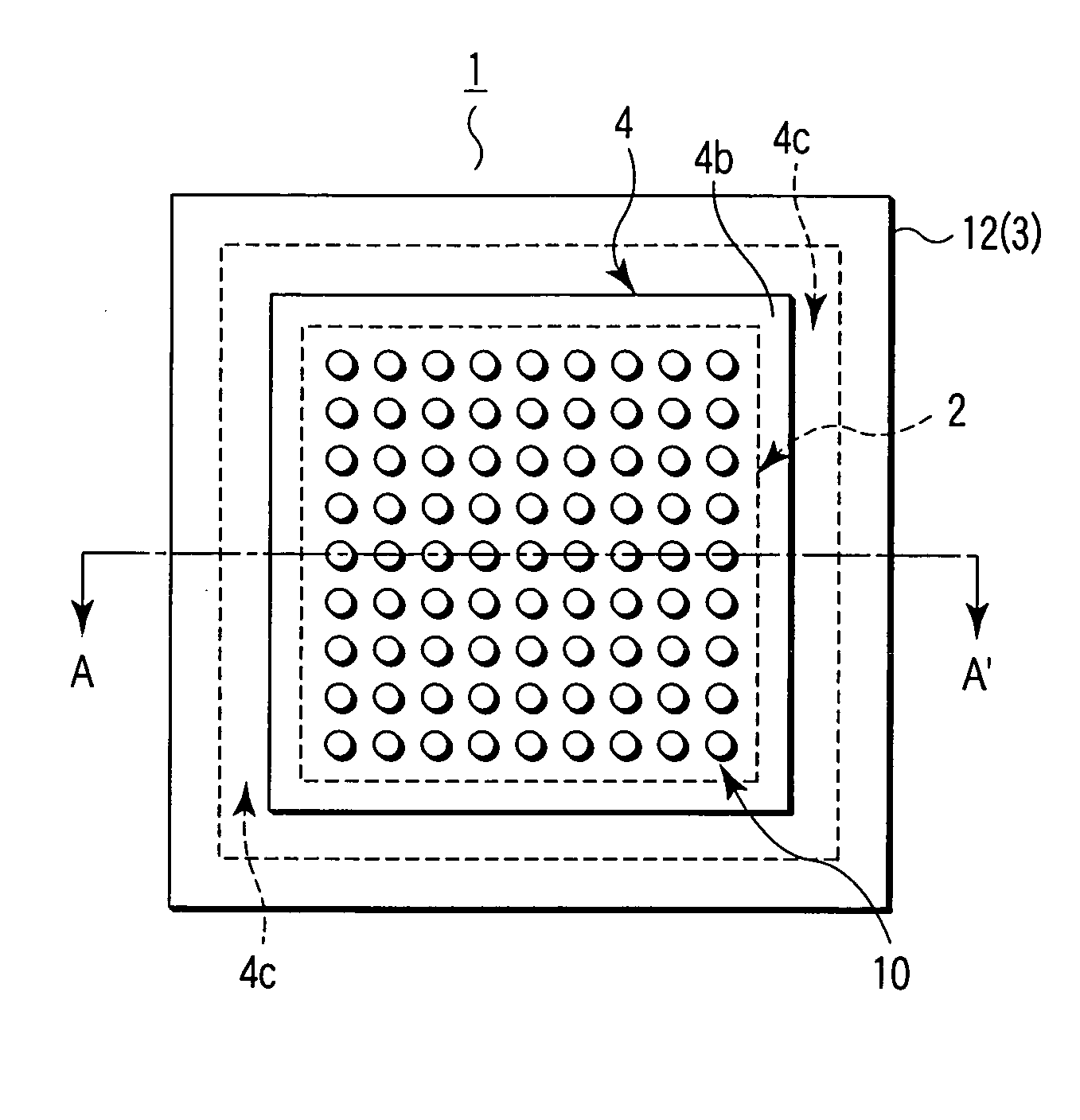
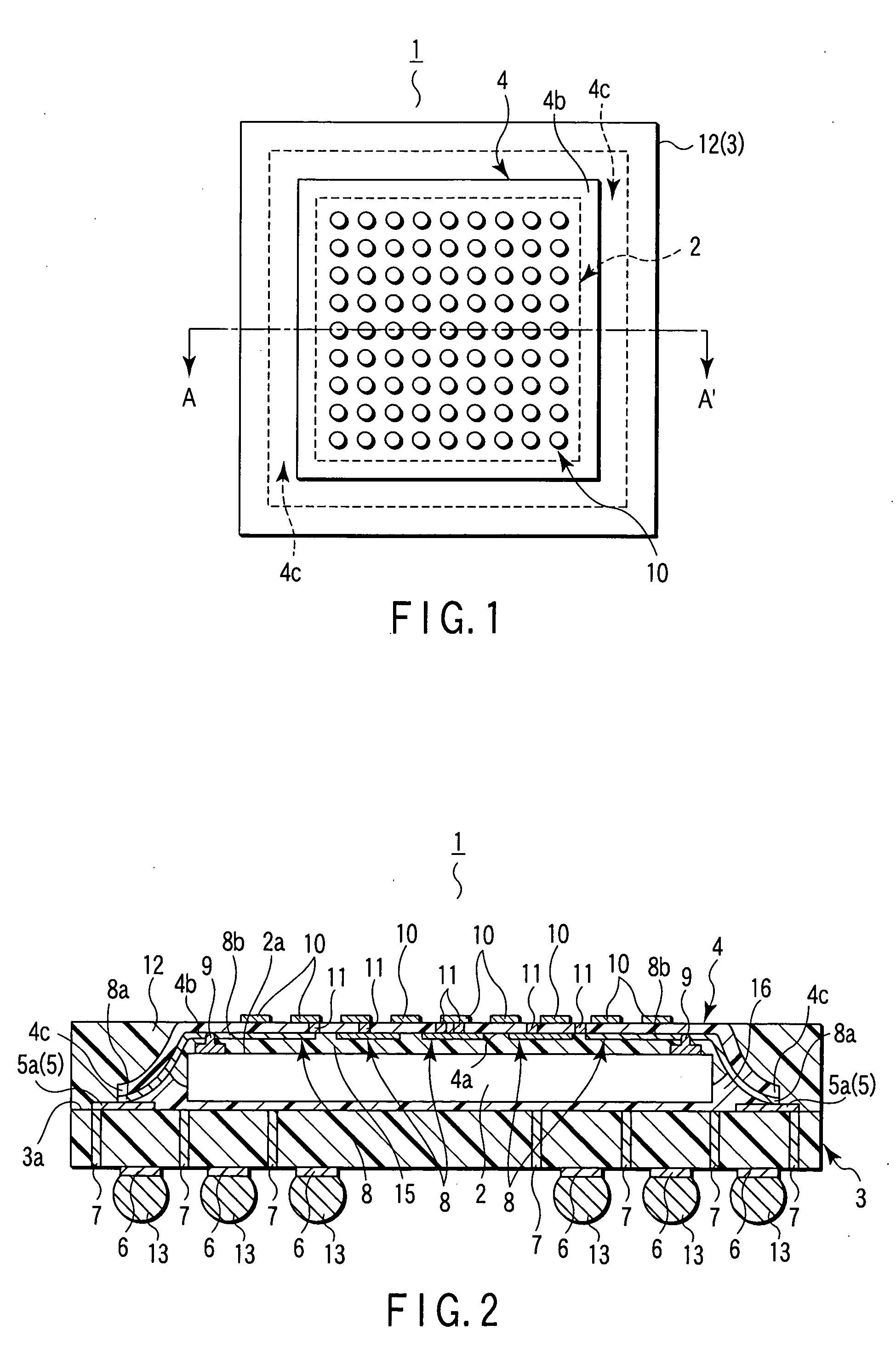
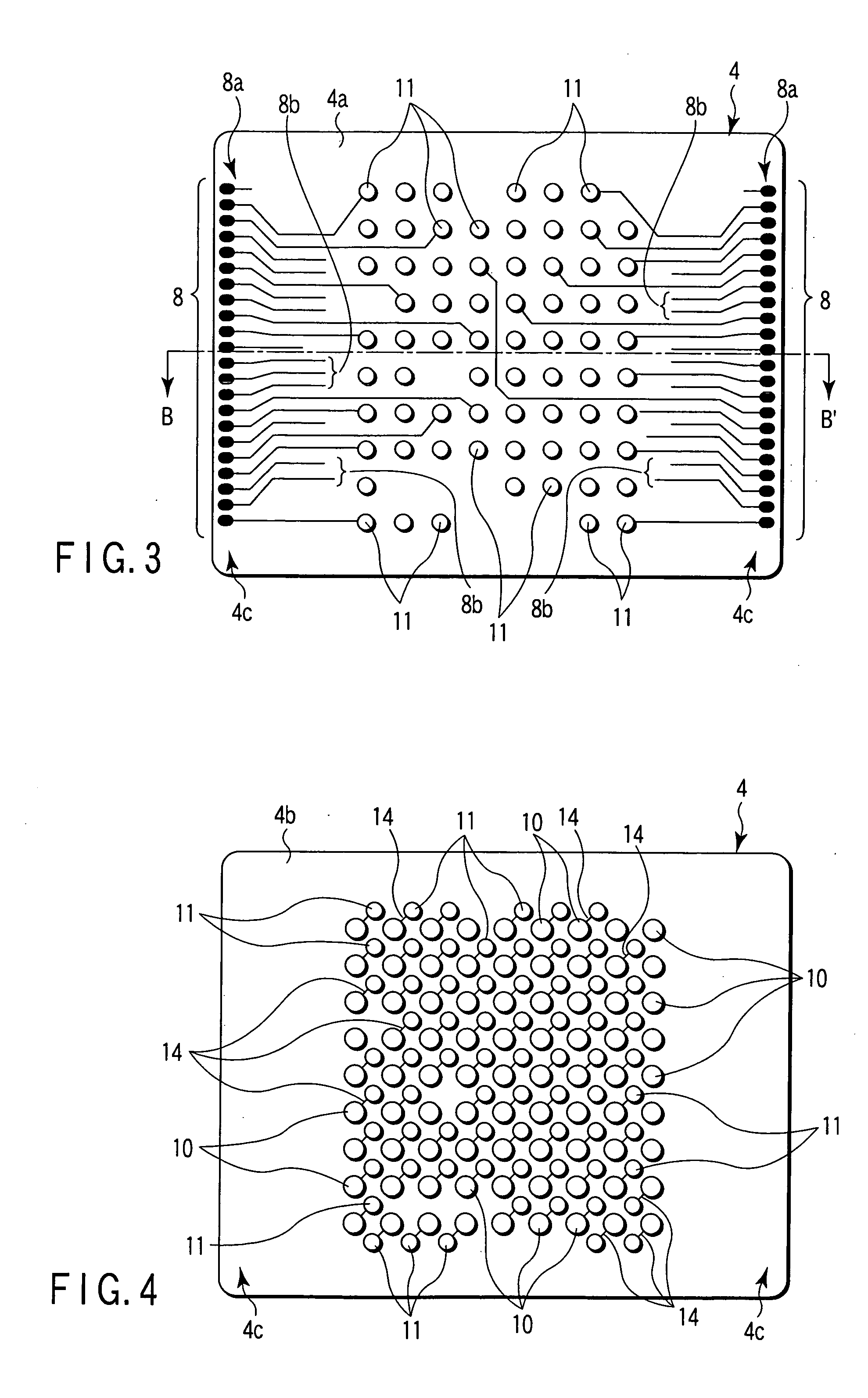
[0058] First, a first embodiment of the present invention will be described with reference to FIGS. 1 to 18. FIG. 1 is a plan view showing a semiconductor device according to the first embodiment seen from a second substrate side of the semiconductor device. FIG. 2 is a sectional view showing the semiconductor device shown in FIG. 1 along a broken line A-A′. FIG. 3 is a plan view showing a second substrate provided in the semiconductor device shown in FIG. 1 seen from the main surface of the second substrate on which a semiconductor element is mounted. FIG. 4 is a plan view showing the second substrate provided in the semiconductor device shown in FIG. 1 seen from the main surface of the second substrate on which external terminals are formed. FIG. 5 is a sectional view showing the second substrate shown in FIG. 3 along a broken line B-B′. FIG. 6 is a plan view showing the second substrate on which the semiconductor element is mounted as seen from the main surface of the second subs...

second embodiment

[0087] Next, a second embodiment of the present invention will be described with reference to FIGS. 19A and 19B. FIGS. 19A and 19B are sectional views showing the connection portions between the first internal wirings provided on the first substrate and the second internal wirings provided on the second substrate in the semiconductor device of the present embodiment. It is to be noted that the same part as that of the first embodiment is denoted with the same reference numerals, and the detailed description is omitted.

[0088] The present embodiment is different from the first embodiment only in a method of connecting the connection terminals 5a of the first internal connection wirings 5 provided on the circuit substrate 3 to the connection terminals 8a of the second internal connection wirings 8 provided on the flexible substrate 4, and the other respect is similar to that of the first embodiment. The present embodiment will be described concretely hereinafter.

[0089] As shown in FI...

third embodiment

[0091] Next, a third embodiment of the present invention will be described with reference to FIGS. 20A and 20B. FIGS. 20A and 20B are sectional views showing the connection portions between the first internal wirings provided on the first substrate and the second internal wirings provided on the second substrate in the semiconductor device of the present embodiment. It is to be noted that the same part as that of the first embodiment is denoted with the same reference numerals, and the detailed description is omitted.

[0092] The present embodiment is different from the first and second embodiments only in the method of connecting the connection terminals 5a of the first internal connection wirings 5 provided on the circuit substrate 3 to the connection terminals 8a of the second internal connection wirings 8 provided on the flexible substrate 4, and the other respects are similar to those of the first and second embodiments. The present embodiment will be described concretely herein...


PUM


Abstract

There is here disclosed a semiconductor device comprising a semiconductor element, a first substrate disposed to face one side of the element, being provided first internal wirings on a main surface, and being provided first external wirings connected to the respective first internal wirings on another main surface, and a second substrate formed to be larger than the element by a material having flexibility, being disposed to face another side of the element, being provided second internal wirings having one-end portions extended to edges of a main surface, and the one-end portions connected to the first internal wirings with being bent toward the first substrate together with the edges, being mounted the element having an electrode connected to some of the second internal wirings on the main surface, and being provided external terminals connected to some of the second internal wirings on a middle of another main surface.

Description

CROSS-REFERENCE TO RELATED APPLICATIONS [0001] This application is based upon and claims the benefit of priority from prior Japanese Patent Application No. 2004-006787, filed Jan. 14, 2004, the entire contents of which are incorporated herein by reference. BACKGROUND OF THE INVENTION [0002] 1. Field of the Invention [0003] The present invention relates to a mounting technique of a semiconductor device, particularly to a semiconductor device whose variations of performances and properties can be increased in a semiconductor device on which one or a plurality of semiconductor elements are mounted and to which another semiconductor device, a passive component and the like are added, and a manufacturing method for the semiconductor device. [0004] 2. Description of the Related Art [0005] As a technique for mounting another semiconductor device onto a certain semiconductor device, several devices, structures, constitutions, and manufacturing methods have heretofore been proposed. The tech...

Claims


Application Information

Patent Timeline
Patent Type & Authority Applications(United States)
IPC IPC(8): H01L21/56H01L21/60H01L23/12H01L23/16H01L23/31H01L23/498H01L25/10H01L25/11H01L25/18
CPCH01L21/565H01L2924/01006H01L23/3128H01L23/49833H01L23/49838H01L24/86H01L24/97H01L25/105H01L2224/16225H01L2224/2402H01L2224/24226H01L2224/24998H01L2224/32225H01L2224/48227H01L2224/48235H01L2224/73265H01L2224/97H01L2924/01029H01L2924/01033H01L2924/01078H01L2924/01079H01L2924/01082H01L2924/15311H01L23/16H01L2924/01005H01L24/48H01L2924/014H01L2224/82007H01L2225/1058H01L2225/1041H01L2225/1023H01L2224/82H01L2924/00H01L2924/181H01L2924/00014H01L2224/45144H01L24/45H01L24/50H01L2924/00012H01L2224/45015H01L2924/207F25B2600/2507F25B2400/075F25B41/20
Inventor YOKOI, TETSUYA
Owner KIOXIA CORP
Why Eureka
Try Eureka