Method for manufacturing semiconductor device

Active Publication Date: 2005-06-16
ABLIC INC
View PDF6 Cites 67 Cited by
  • Summary
  • Abstract
  • Description
  • Claims
  • Application Information

AI Technical Summary

Benefits of technology

[0045] An embodiment of the present invention will be described in detail later. To explain it in brief, as shown in FIG. 1, variations of the semiconductor device are copied to the monitor element 200 (FIG. 4) in course of manufacture (FIG. 1, Step C), a quality of the half-completed semiconductor device is checked (FIG. 1, Step F), a quality of the completed semiconductor device is estimated based on the measured information (FIG. 1, Step G1), the manufacturing conditions of a variation reduction step in the subsequent manufacturing process are set in an analog fashion based on the estimated information (FIG. 1, Step G2), and the variations in electric characteristics are reduced under the newly set manufacturing conditions to complete the manufacture of the semiconductor device (FIG. 1, Step H). Variations in electric characteristics of the semiconductor device in course of manufacture can thus be reduced considerably. In other words, according to the present invention, the variations of the semiconductor d

Problems solved by technology

Upon manufacturing any products, product-to-product variation (production variation) impairs uniformity in product characteristics (inclusive of function, performance, and shape).
To prevent it, a manufacturer faces an agonizing choice between relaxing a production specification to keep a production yield at a certain level (decrease in quality) and complying with a product specification to thereby cause reduction in production yield (increase in cost).
Looking closer, the manufacturing process is very complicated and consists of well over 100 steps.
However, the conventional manufacturing method

Method used


Image

  • Method for manufacturing semiconductor device
  • Method for manufacturing semiconductor device
  • Method for manufacturing semiconductor device

Examples


embodiment

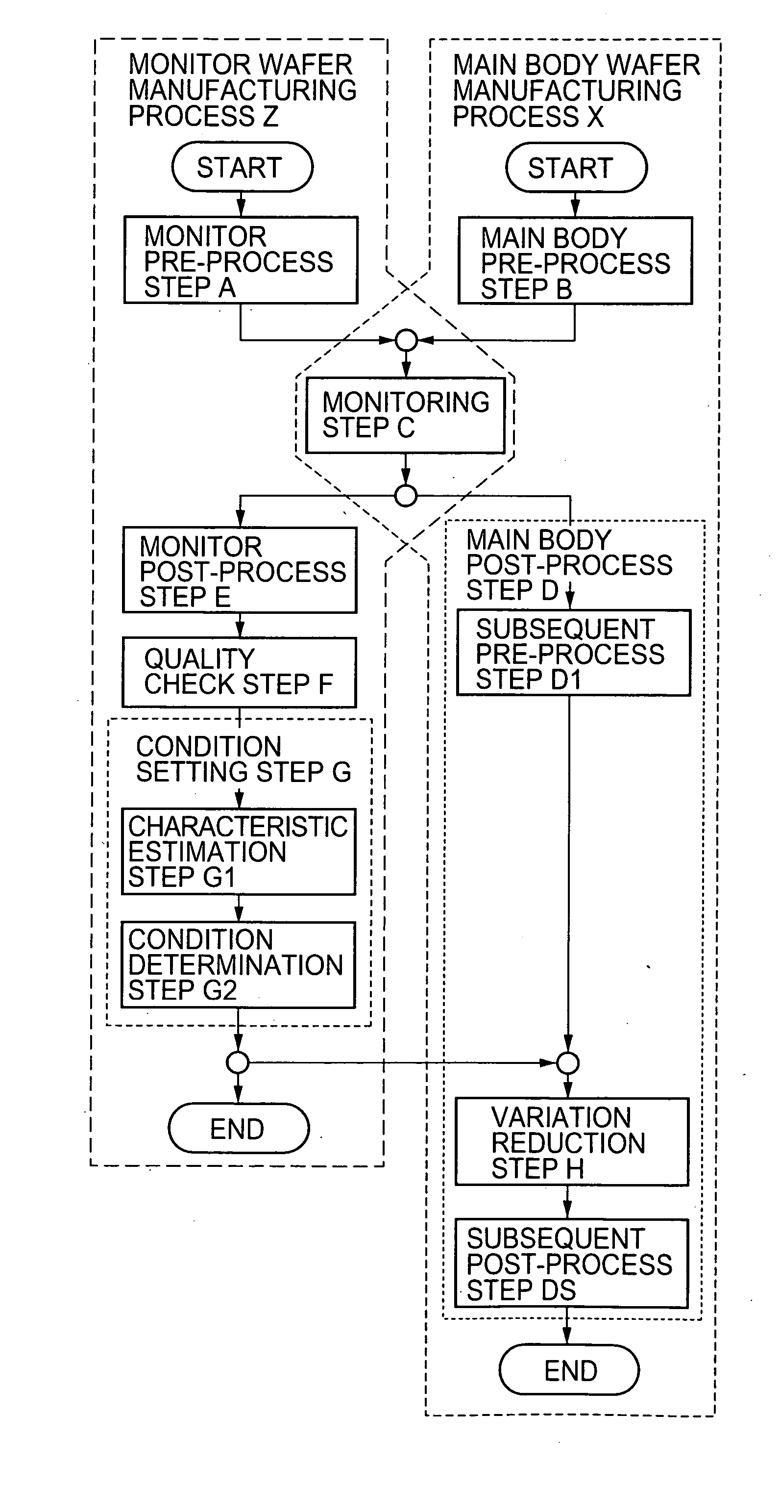
[0079] The monitor wafer manufacturing process Z as a feature of the present invention includes: a monitor wafer pre-process step (FIG. 1, Step A); a step of copying characteristics of a main body wafer by simultaneously processing the main body wafer and monitor wafer (FIG. 1, Step C); a monitor post-process step for the monitor element 200 (FIG. 1, Step E); a step of measuring characteristics of the monitor element 200 (FIG. 1, Step F); and a step of setting manufacturing conditions in the variation reduction step H (FIG. 1, Step G). Here, the monitoring step C of copying the quality of the half-completed main body wafer on the monitor wafer aims at simultaneously processing the main body wafer and the monitor wafer in the same apparatus. In this embodiment, a MOS diode shown in FIG. 4 is used as the monitor element 200 where the quality of the half-completed semiconductor device is copied in the monitoring step C. Hereinafter, an embodiment of the feed-forward type manufacturing ...


PUM


Abstract

A manufacturing method for a semiconductor device which is capable of manufacturing the semiconductor device with a high quality in high yields while reducing variations in electric characteristic is disclosed. The manufacturing method according to the present invention includes a main body wafer manufacturing process for manufacturing a wafer on which a semiconductor device to be completed as a product is formed and a monitor wafer manufacturing process for manufacturing a wafer on which a monitor element is formed, the processes sharing a monitoring step alone, the main body wafer manufacturing process including a variation reduction step, the monitor wafer manufacturing process including a quality check step and a condition setting step.

Description

BACKGROUND OF THE INVENTION [0001] 1. Field of the Invention [0002] The present invention relates to a manufacturing method for a semiconductor device. In particular, the invention relates to a manufacturing method for a semiconductor device including a method of monitoring halfway through a manufacturing process of the semiconductor device and a method of reflecting monitoring information to its subsequent manufacturing process. [0003] 2. Description of the Related Art [0004] Upon manufacturing any products, product-to-product variation (production variation) impairs uniformity in product characteristics (inclusive of function, performance, and shape). To prevent it, a manufacturer faces an agonizing choice between relaxing a production specification to keep a production yield at a certain level (decrease in quality) and complying with a product specification to thereby cause reduction in production yield (increase in cost). Under such circumstances, regarding a manufacturing metho...

Claims


Application Information

Patent Timeline
IPC IPC(8): H01L21/66G01R31/26H01L21/00H01L21/02
CPCH01L22/14H01L22/20H01L2924/0002H01L2924/00
Inventor ISHII, KAZUTOSHIOSANAI, JUNKITAJIMA, YUICHIROMINAMI, YUKIMASAUEMURA, KEISUKEWAKE, MIWA
Owner ABLIC INC
Why Eureka
Try Eureka