Method of forming a silicon-rich nanocrystalline structure by an atomic layer deposition process and method of manufacturing a non-volatile semiconductor device using the same

a nanocrystalline structure and atomic layer deposition technology, applied in the direction of nanoinformatics, polycrystalline material growth, crystal growth process, etc., can solve the problems of inferior reliability of the tunnel dielectric layer, hot electrons in the floating gate may come out through defects, and the relationship between electron retention and the defect, so as to improve the programming and erasing operation, the effect of high silicon conten

Active Publication Date: 2008-09-02
SAMSUNG ELECTRONICS CO LTD
View PDF26 Cites 66 Cited by
  • Summary
  • Abstract
  • Description
  • Claims
  • Application Information

AI Technical Summary

Benefits of technology

[0019]Example embodiments of the present invention provide a method of forming a silicon-rich nanocrystalline structure having a good step coverage and an improved variation of silicon content therein by an atomic layer deposition process.
[0049]According to the present invention, a silicon-rich nanocrystalline structure may include at least one silicon-rich insulation layer and at least one silicon nanocrystalline layer alternately formed on an object or a substrate or a tunnel dielectric layer. The at least one silicon-rich insulation layer and the at least one silicon nanocrystalline layer may be formed by atomic layer deposition processes using first gases capable of widening a silicon content in a wide range. In addition, the silicon-rich nanocrystalline structure may have a high silicon content and a good step coverage. When the silicon-rich nanocrystalline structure is employed as a charge trapping structure of a non-volatile semiconductor device, the non-volatile semiconductor device may have improved programming and erasing operations and also an enhanced data retention capability.

Problems solved by technology

However, there are problems in relation to the electron retention in the non-volatile semiconductor memory device having the vertically stacked gate structure.
When defects such as pinholes exist in the tunnel dielectric layer, the hot electrons in the floating gate may come out through the defects.
However, the formation of the tunnel dielectric layer having the thin thickness causes difficulty in manufacturing uniform semiconductor devices and causes inferior reliability of the tunnel dielectric layer.
Since the silicon nanocrystals are electrically separated, electro-migration between the silicon nanocrystals may be restricted.
Thus, there is a limit to increase a silicon content of the silicon-rich oxide layer.
Meanwhile, in the formation of the silicon-rich oxide layer on a semiconductor substrate having a pattern thereon through the PECVD process, the silicon-rich oxide layer may have a poor step coverage due to a plasma employed in the PECVD process.
In the formation of the silicon-rich oxide layer by the silicon implantation process in which silicon atoms are injected into an oxide layer, a leakage current may be generated because of damages to the silicon-rich oxide layer caused by the injection of the silicon atoms.
Further, it is very difficult to control densities and sizes of the silicon nanocrystals in the silicon-rich oxide layer.

Method used


Image

  • Method of forming a silicon-rich nanocrystalline structure by an atomic layer deposition process and method of manufacturing a non-volatile semiconductor device using the same
  • Method of forming a silicon-rich nanocrystalline structure by an atomic layer deposition process and method of manufacturing a non-volatile semiconductor device using the same
  • Method of forming a silicon-rich nanocrystalline structure by an atomic layer deposition process and method of manufacturing a non-volatile semiconductor device using the same

Examples


Embodiment Construction

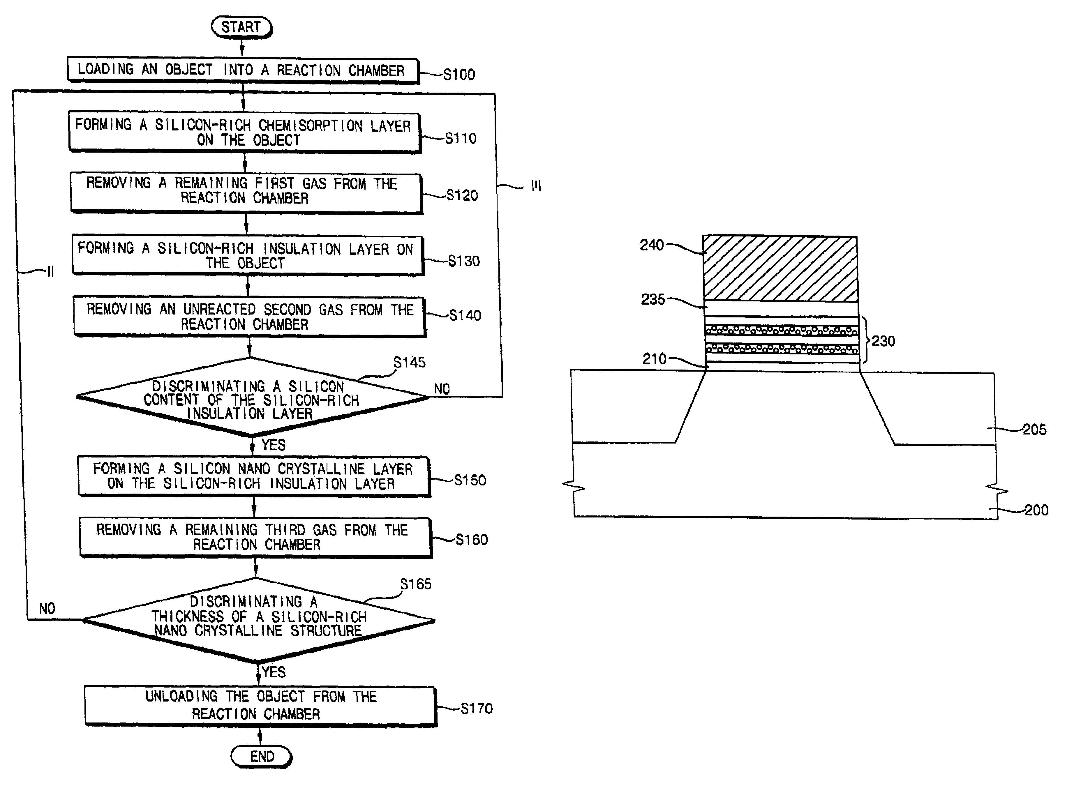
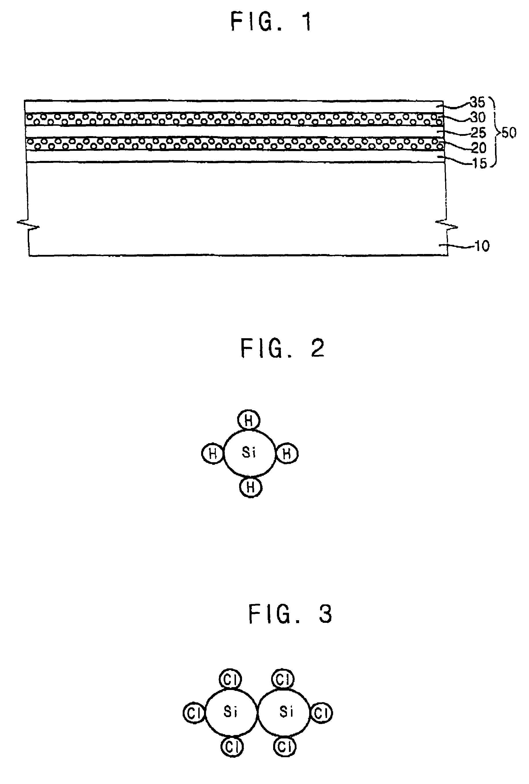
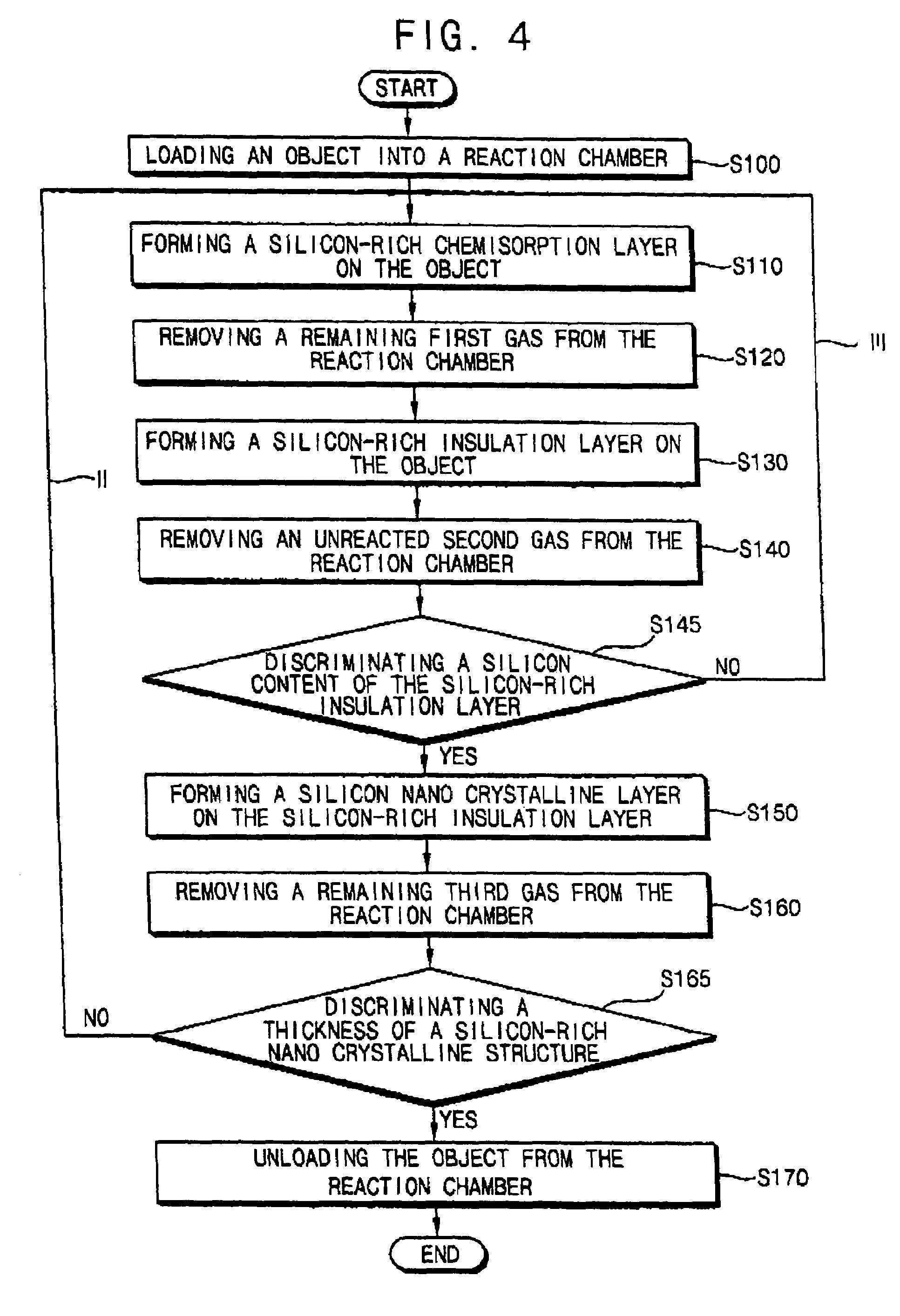
[0057]The present invention is described more fully hereinafter with reference to the accompanying drawings, in which example embodiments of the present invention are shown. The present invention may, however, be embodied in many different forms and should not be construed as limited to the example embodiments set forth herein. Rather, these embodiments are provided so that this disclosure will be thorough and complete, and will fully convey the scope of the present invention to those skilled in the art. In the drawings, the size and relative sizes of layers and regions may be exaggerated for clarity.

[0058]It will be understood that when an element or layer is referred to as being “on”, “connected to” or “coupled to” another element or layer, it can be directly on, connected or coupled to the other element or layer or intervening elements or layers may be present. In contrast, when an element is referred to as being “directly on,”“directly connected to” or “directly coupled to” anot...


PUM

PropertyMeasurementUnit
temperatureaaaaaaaaaa
voltageaaaaaaaaaa

Abstract

In a method of forming a silicon-rich nanocrystalline structure by an ALD process, a first gas including a first silicon compound is provided onto an object to form a silicon-rich chemisorption layer on the object. A second gas including oxygen is provided onto the silicon-rich chemisorption layer to form a silicon-rich insulation layer on the object. A third gas including a second silicon compound is provided onto the silicon-rich insulation layer to form a silicon nanocrystalline layer on the silicon-rich insulation layer. The first gas, the second gas and the third gas may be repeatedly provided to alternately form the silicon-rich nanocrystalline structure having a plurality of silicon-rich insulation layers and a plurality of silicon nanocrystalline layers on the object.

Description

CROSS-REFERENCE TO RELATED APPLICATION[0001]This application claims priority under 35 USC §7 119 to Korean Patent Application No. 2005-69371 filed on Jul. 29, 2005 and Korean Patent Application No. 2006-44141 filed on May 17, 2006, the contents of which are herein incorporated by reference in their entirety for all purposes.BACKGROUND OF THE INVENTION[0002]1. Field of the Invention[0003]Example embodiments of the present invention relates to a method of forming a silicon-rich nanocrystalline structure and a method of manufacturing a non-volatile semiconductor device using the same. More particularly, example embodiments the present invention relates to a method of forming a silicon-rich nanocrystalline structure by an atomic layer deposition (ALD) process, and a method of manufacturing a non-volatile semiconductor device using the same.[0004]2. Description of the Related Art[0005]Generally, semiconductor memory devices are classified into volatile semiconductor memory devices such a...

Claims


Application Information

Patent Timeline
Patent Type & Authority Patents(United States)
IPC IPC(8): H01L21/20H01L21/36
CPCB82Y10/00C23C16/308C23C16/401H01L29/42328H01L21/28273H01L21/3141H01L21/32055C23C16/45529Y10S438/962H01L29/40114H01L21/02164H01L21/0214H01L21/0228H01L21/02211H01L21/02337
Inventor YANG, SANG-RYOLJOO, KYONG-HEEYEO, IN-SEOKHWANG, KI-HYUNLIM, SEUNG-HYUN
Owner SAMSUNG ELECTRONICS CO LTD
Why Eureka
Try Eureka