

Low profile package having multiple die
a technology of semiconductor devices and dies, applied in semiconductor devices, semiconductor/solid-state device details, electrical equipment, etc., can solve the problems of increasing part and assembly costs for end applications, reducing the cost, size and weight of high-volume consumer applications, and prior art device packages not always suitable, so as to reduce the height of the device package, reduce the cost of part and assembly costs, and the effect of low profil
- Summary
- Abstract
- Description
- Claims
- Application Information
AI Technical Summary
Benefits of technology
Problems solved by technology
Method used
Image

Examples
Embodiment Construction
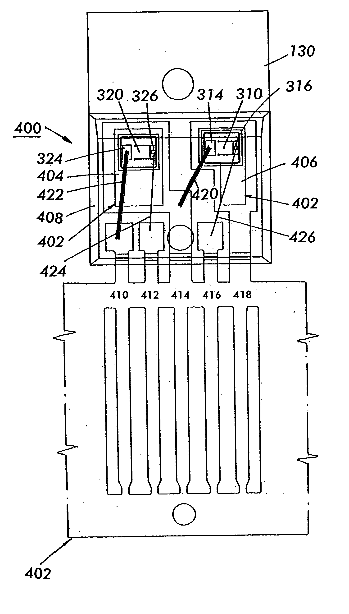
[0032] Referring now to FIGS. 4 and 5, an example semiconductor device package 400 in accordance with an example embodiment of the present invention is shown. Preferably, device package 400 is similar to device package 100 of the prior art and has a lead frame 402 and a number of lead terminals 410-418 that are substantially similar to those of package 100. However, the lead frame according to this embodiment of the invention now includes two distinct die pads 404 and 406 for receiving at least two semiconductor die, contrary to the single die pad of package 100. The semiconductor die can be MOSFET die, diodes, IGBTs, or the like or some combination thereof. As such, example package 400 according to this embodiment of the invention is a low profile semiconductor device package that provides for multiple semiconductor die that can form a circuit.
[0033] More specifically, referring to FIG. 4, the example package 400 according to this example embodiment of the invention includes five ...
PUM
 Abstract
Description
Claims
Application Information