Output circuit, liquid crystal driving circuit, and liquid crystal driving method

a technology of liquid crystal driving circuit and output circuit, which is applied in the direction of instruments, static indicating devices, etc., can solve the problems of limiting the speed with which the liquid crystal panel can be driven, lowering image quality, and impairing accuracy

Active Publication Date: 2005-07-14
LAPIS SEMICON CO LTD
View PDF4 Cites 31 Cited by
  • Summary
  • Abstract
  • Description
  • Claims
  • Application Information

AI Technical Summary

Benefits of technology

[0009] An object of the present invention is to provide an output circuit in which an impedance conversion element, switchably

Problems solved by technology

Although the potential difference diminishes and eventually disappears as the capacitors approach and eventually reach the intended charge level, the potential difference slows the approach, thereby limiting the speed with which the liquid crystal panel can be driven.
A further problem is that variations in wiring resistance due to variations in the on-resistance of the analog switches and the wiri

Method used


Image

  • Output circuit, liquid crystal driving circuit, and liquid crystal driving method
  • Output circuit, liquid crystal driving circuit, and liquid crystal driving method
  • Output circuit, liquid crystal driving circuit, and liquid crystal driving method

Examples


second embodiment

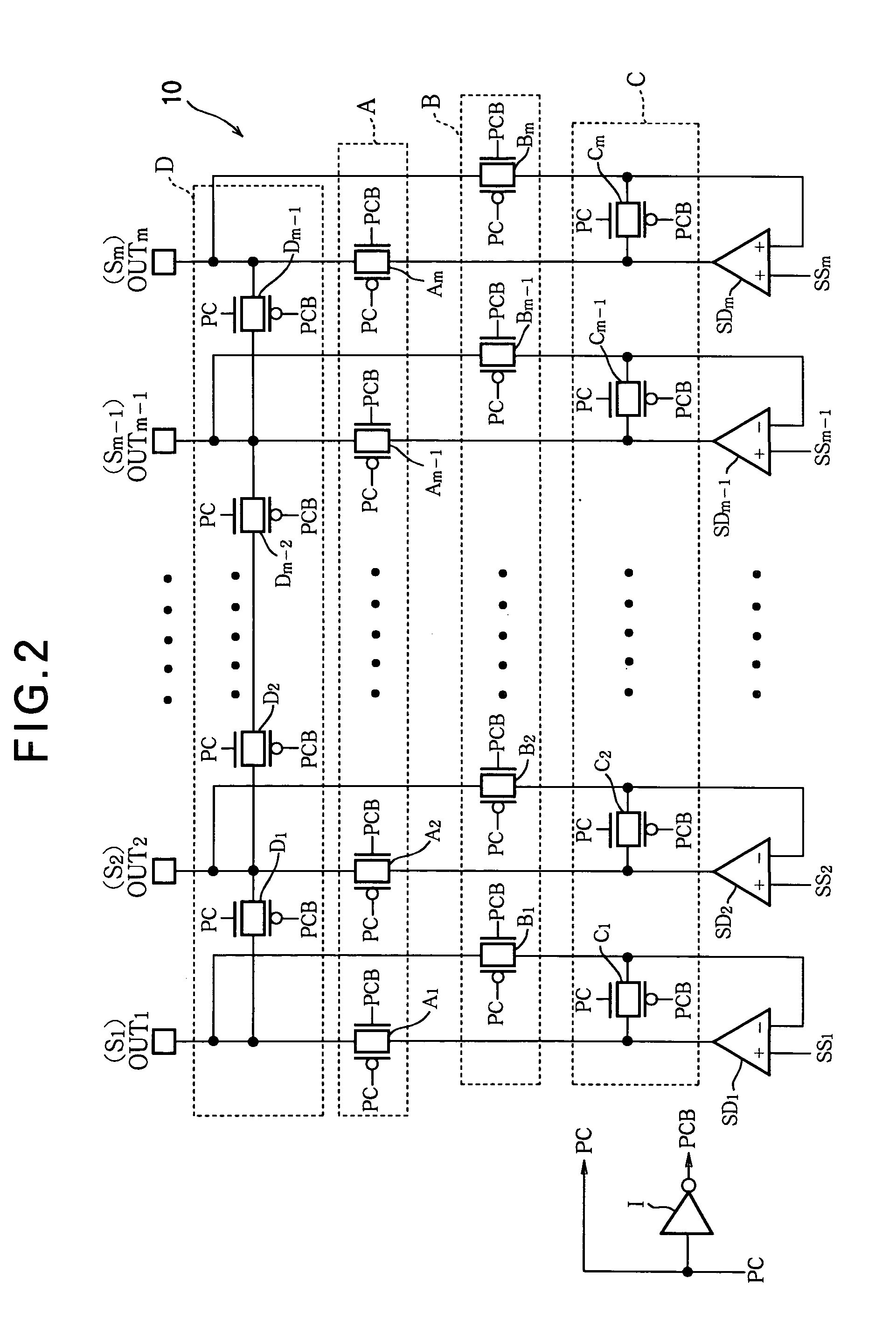
[0055] Referring to FIG. 5, the source driving circuit 20 in the second embodiment comprises m source drivers SD1, SD2, . . . , SDm, an A-group of analog switches that control output paths, a B-group of analog switches that control first feedback paths, a C-group of analog switches that control second feedback paths, an E-group of analog switches that control precharging, an a-group of protective resistors, a b-group of feedback resistors, a group of m output terminals OUT1, OUT2, . . . , OUTm, and an inverter I, where m is an even number.

[0056] The source driving circuit 20 accordingly adds protective resistors and feedback resistors to the source driving circuit 10 in the first embodiment, and alters the group of analog switches that control precharging. The source driving circuit 20 in the second embodiment also arranges the feedback paths during the driving period so that they branch from points following the protective resistors.

[0057] The E-group of analog switches comprises...

third embodiment

[0078] Referring to FIG. 6, the source driving circuit 30 in the third embodiment comprises m source drivers SD1, SD2, . . . , SDm, an A-group of analog switches that control output paths, a B-group of analog switches that control first feedback paths, a C-group of analog switches that control second feedback paths, an F-group of analog switches that control precharging, a group of m output terminals OUT1, OUT2, . . . , OUTm, and an inverter I, where m is an arbitrary integer equal to or greater than two.

[0079] The source driving circuit 30 in the third embodiment accordingly alters the group of analog switches that control precharging in the source driving circuit 10 (see FIGS. 1 and 2) in the first embodiment.

[0080] The F-group of analog switches comprises m analog switches (MOS switches) F1, F2, . . . , Fm. Analog switch Fi is connected between the i-th output terminal OUTi (source line Si) of the source driving circuit 30 and the common voltage Vcom (the potential of the commo...


PUM


Abstract

An output circuit for driving a signal line in, for example, a liquid crystal display panel has an impedance conversion element that generates an output signal from an input signal and a feedback signal. During output periods, a first switch conducts the output signal to the output terminal of the output circuit and a second switch conducts the output signal from the output terminal back to the impedance element as the feedback signal. During non-output periods, the first and second switches are switched off and a third switch conducts the output signal back to the impedance element as the feedback signal from a point between the impedance conversion element and the first switch. This dual feedback scheme enables the signal line to be precharged during non-output periods while avoiding loss of driving speed and accuracy during output periods.

Description

BACKGROUND OF THE INVENTION [0001] 1. Field of the Invention [0002] The present invention relates to an output circuit employing feedback control, a liquid crystal driving circuit that uses the output circuit to drive a liquid crystal panel, and a liquid crystal driving method that uses the output method of the output circuit to drive a liquid crystal panel. [0003] 2. Description of the Related Art [0004] As disclosed in Japanese Unexamined Patent Application Publication No. 11-30975, the driving speed of a liquid crystal display panel having source lines driven by operational amplifiers can be increased by precharging the source lines. The source lines are precharged by disconnecting them from their drivers (the operational amplifiers) and either interconnecting the source signal lines, or connecting them to a fixed potential such as the common-voltage potential of the liquid crystal display panel. [0005]FIG. 8 illustrates the former precharging scheme in a conventional liquid crys...

Claims


Application Information

Patent Timeline
IPC IPC(8): G09G3/20G02F1/133G09G3/36
CPCG09G3/3614G09G2320/0252G09G2310/0248G09G3/3688
Inventor HIRAMA, ATSUSHI
Owner LAPIS SEMICON CO LTD
Why Eureka
Try Eureka