

Wide dynamic range operations for imaging
- Summary
- Abstract
- Description
- Claims
- Application Information
AI Technical Summary
Problems solved by technology
Method used
Image

Examples
Embodiment Construction
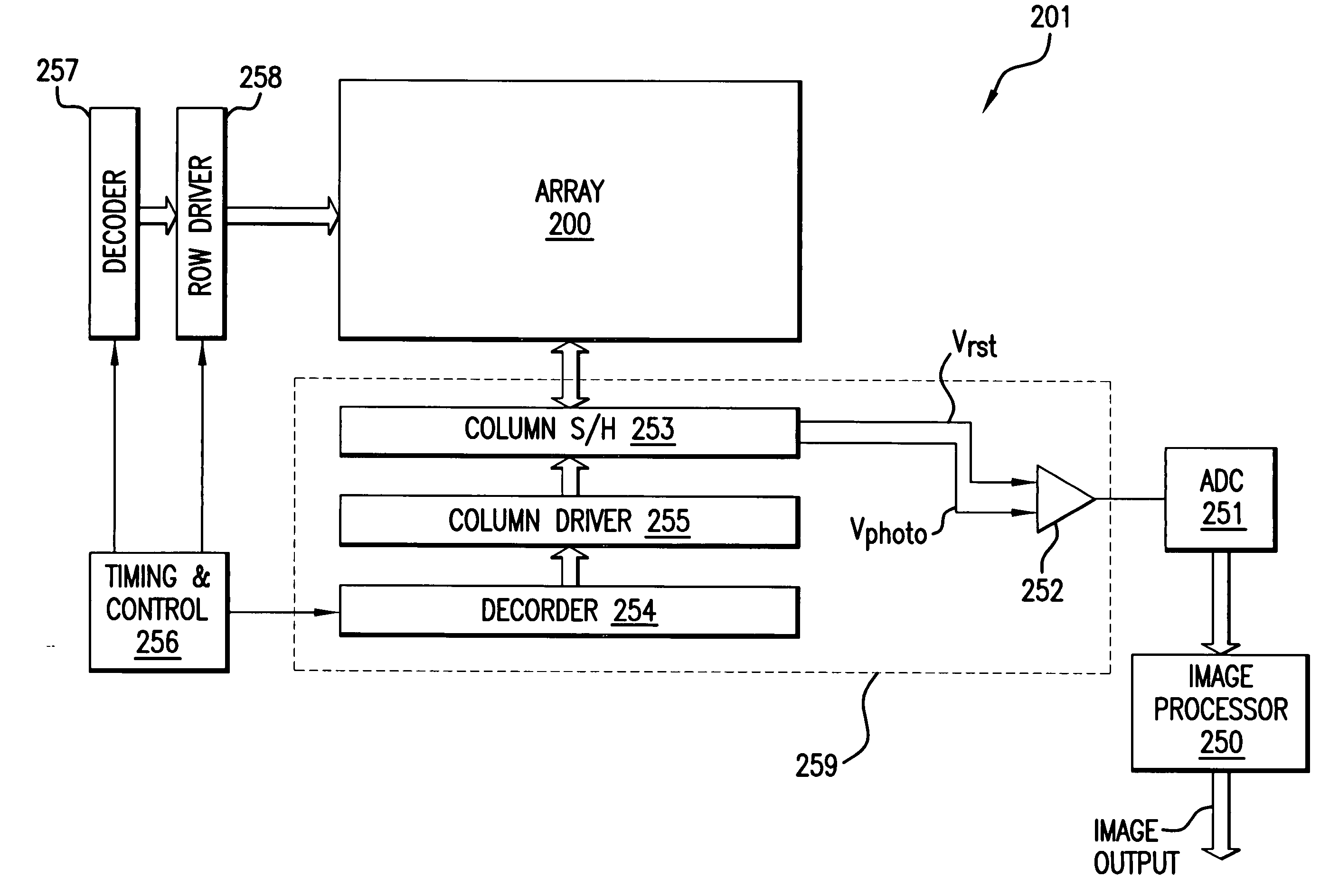
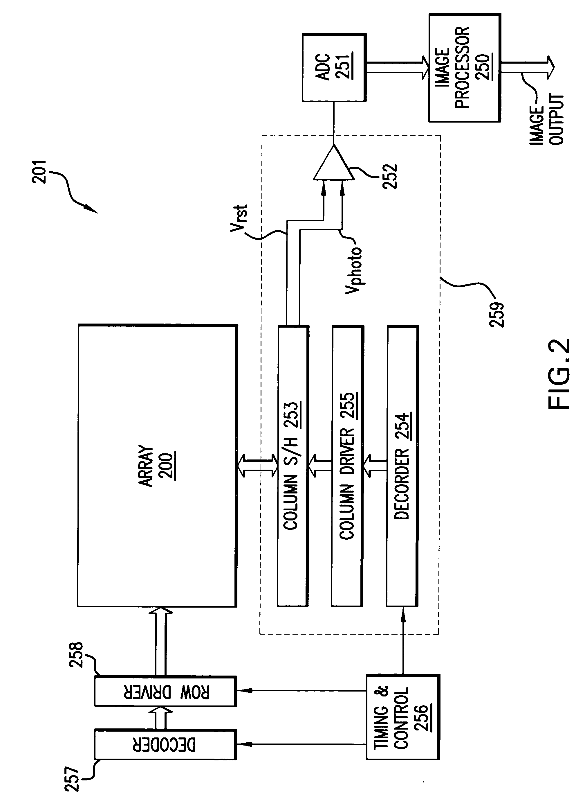
[0038] In the following detailed description, reference is made to the accompanying drawings, which form a part hereof and illustrate specific embodiments in which the invention may be practiced. In the drawings, like reference numerals describe substantially similar components throughout the several views. These embodiments are described in sufficient detail to enable those skilled in the art to practice the invention, and it is to be understood that other embodiments may be utilized, and that structural, logical and electrical changes may be made without departing from the spirit and scope of the present invention.
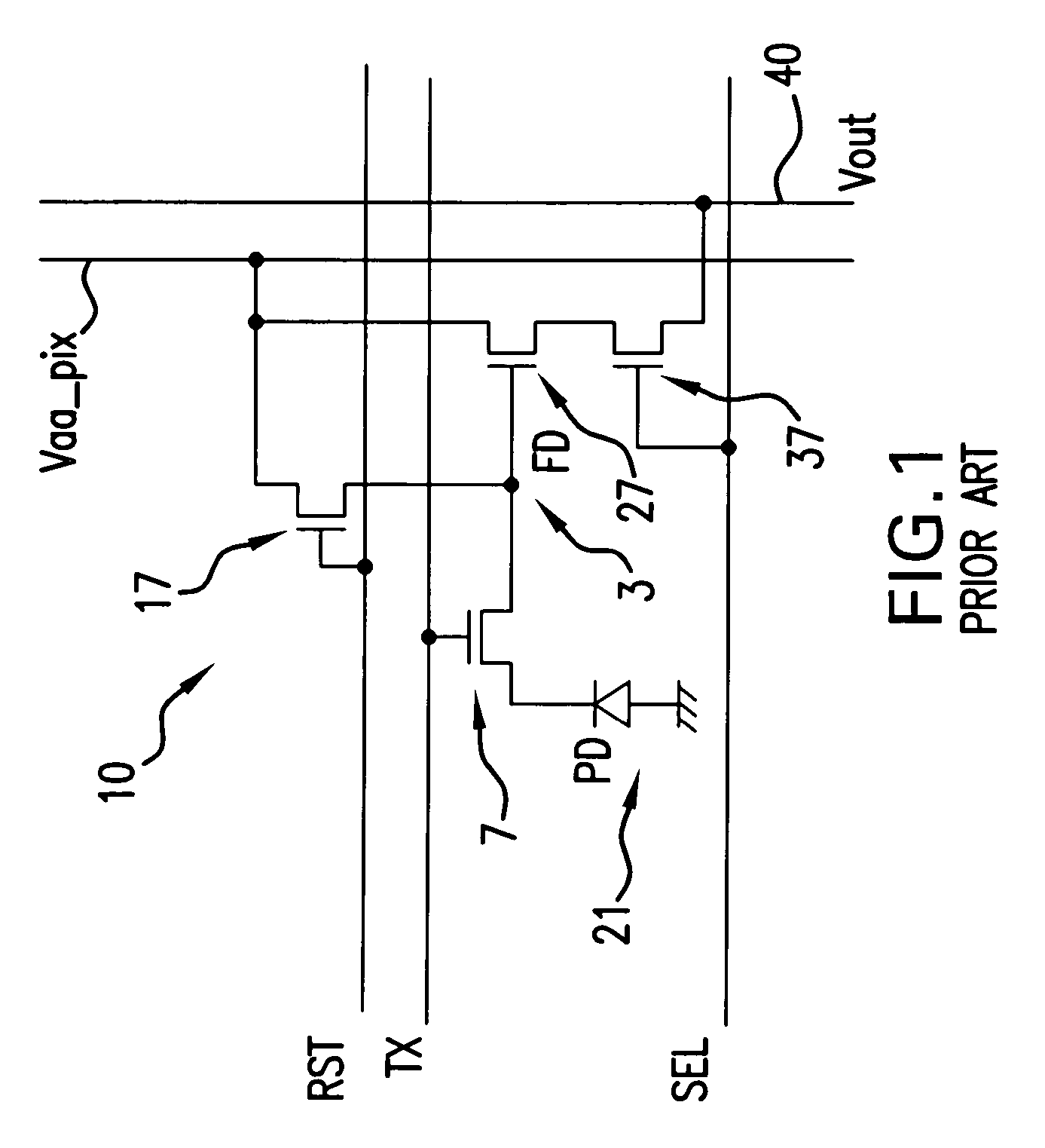
[0039] The term “pixel” or “pixel cell” refers to a picture element unit cell containing a photo-conversion device and associated transistors or other circuitry that convert electromagnetic radiation to an electrical signal. For purposes of illustration, representative pixel cells are illustrated in the figures and description herein, and typically all pixels in an imag...
PUM
 Abstract
Description
Claims
Application Information