Solid-state imaging device and signal processing circuit

a solid-state imaging and signal processing circuit technology, applied in the direction of radioation control devices, instruments, television systems, etc., can solve the problems of poor shading, achieve the effect of high sensitivity, poor shading, and high-quality captur

Inactive Publication Date: 2005-07-14
SONY CORP
View PDF5 Cites 28 Cited by
  • Summary
  • Abstract
  • Description
  • Claims
  • Application Information

AI Technical Summary

Benefits of technology

[0015] In the solid-state imaging device of the present invention, the sensitivity of a photoelectric conversion region having the highest sensitivity in the peripheral pixel regions is higher than that of a photoelectric conversion region having the highest sensitivity in the central pixel region. Thus, so-called shading caused by more oblique incident light components in the light incident on a peripheral portion of the solid-state imaging device than in a central portion thereof, namely, shading caused by the photoelectric conversion regions having the highest sensitivity in the pixel regions, can be corrected for. Therefore, the solid-state imaging device provides high-quality captured images.
[0016] The signal processing circuit of the present invention corrects for gains of the central pixel region and peripheral pixel regions in accordance with an f value. For example, if the photoelectric conversion regions having the highest sensitivity in the central pixel region and peripheral pixel regions are suppressed from causing shading, the low-sensitivity photoelectric conversion regions may cause worse shading. However, shading caused in the regions other than the photoelectric conversion regions having the highest sensitivity in the pixel regions can be corrected for. Therefore, the solid-state imaging device provides high-quality captured images.

Problems solved by technology

For example, if the photoelectric conversion regions having the highest sensitivity in the central pixel region and peripheral pixel regions are suppressed from causing shading, the low-sensitivity photoelectric conversion regions may cause worse shading.

Method used


Image

  • Solid-state imaging device and signal processing circuit
  • Solid-state imaging device and signal processing circuit
  • Solid-state imaging device and signal processing circuit

Examples


first embodiment

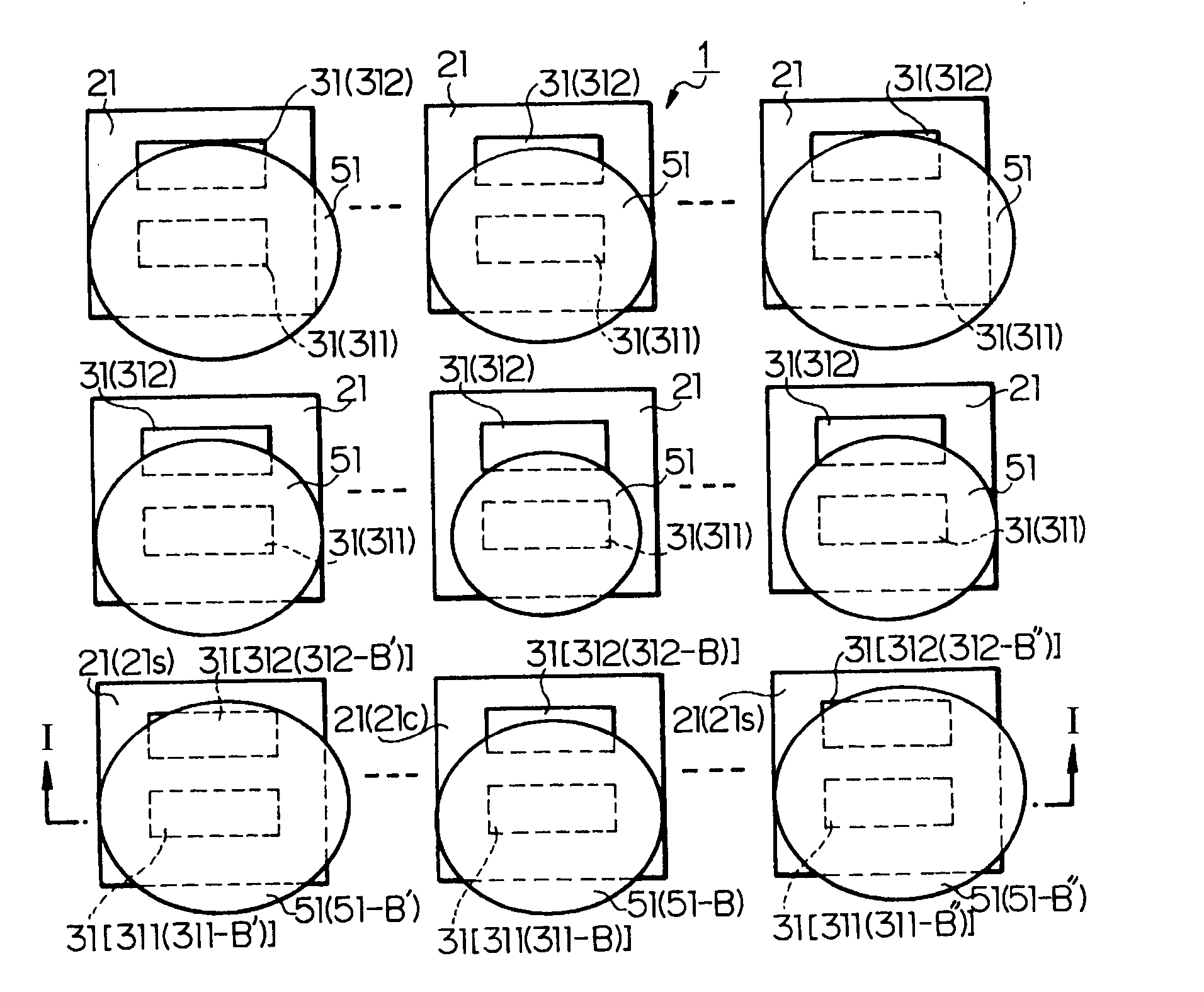
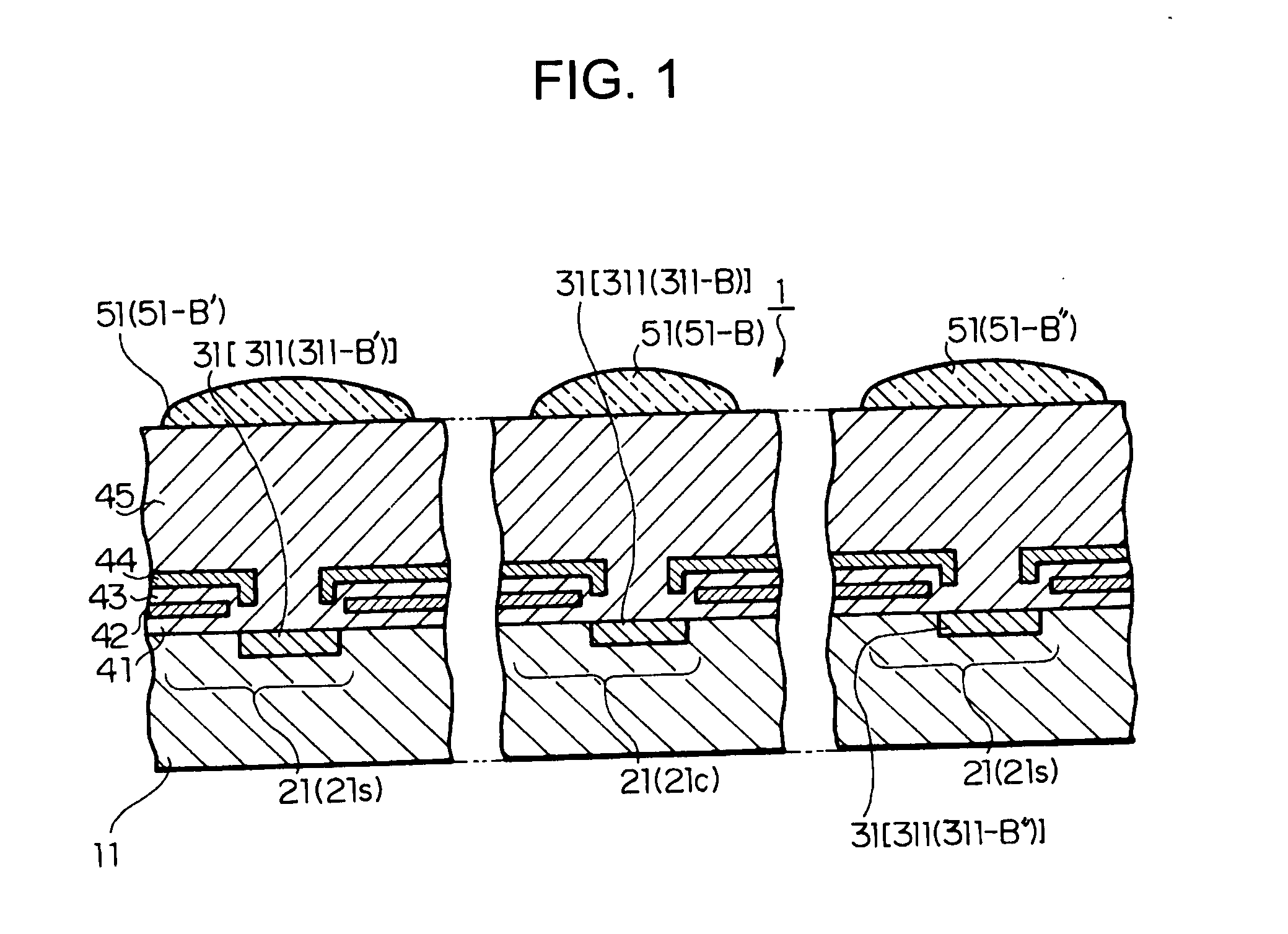
[0023] A solid-state imaging device according to a first embodiment of the present invention will be described with reference to FIGS. 1 and 2. FIG. 2 is a plan view of the solid-state imaging device, and FIG. 1 is a schematic cross-sectional view of the solid-state imaging device, taken along a line I-I of FIG. 2.

[0024] As shown in FIGS. 1 and 2, three or more pixel regions 21 are formed on a semiconductor substrate 11 in at least one direction (in FIG. 2, two directions) of two different directions along a principal surface of the semiconductor substrate 11. Each of the pixel regions 21 includes a plurality of photoelectric conversion regions 31, e.g., two photoelectric conversion regions 31 (311 and 312). The photoelectric conversion regions 311 and 312 have different sensitivities (light sensitivities). The photoelectric conversion region 311 has a higher sensitivity than the photoelectric conversion region 312.

[0025] In this solid-state imaging device, the high-sensitivity ph...

second embodiment

[0036] The first embodiment may cause worse shading in low-sensitivity pixels as a result of shading correction in high-sensitivity pixels. A solid-state imaging device according to a second embodiment of the present invention corrects for worse shading caused in low-sensitivity pixels.

[0037] In the second embodiment, a signal processing circuit (not shown) external to or on the same chip as the solid-state imaging device of the second embodiment corrects for gains of the central pixel region 21c and the peripheral pixel regions 21s shown in FIGS. 1 and 2 in accordance with the f values of the condenser lenses 51.

[0038] In the solid-state imaging device, for example, if the high-sensitivity photoelectric conversion regions 311 in the central and peripheral pixel regions 21c and 21s of the pixel regions 21 shown in FIGS. 1 and 2 are suppressed from causing shading, the low-sensitivity photoelectric conversion regions 312 may cause worse shading. In this case, the signal processing ...

third embodiment

[0039]FIG. 3 is a block diagram of a signal processing circuit 5 according to a third embodiment of the present invention.

[0040] As shown in FIG. 3, the signal processing circuit 5 includes an analog-to-digital (AD) conversion circuit 51H for performing AD conversion on a signal SH output from a high-sensitivity photoelectric conversion region, and an AD conversion circuit 51L for performing AD conversion on a signal SL output from a low-sensitivity photoelectric conversion region.

[0041] The AD conversion circuit 51H is connected to a memory 52H for temporarily storing the digital signal converted by the AD conversion circuit 51H, and the AD conversion circuit 51L is connected to a memory 52L for temporarily storing the digital signal converted by the AD conversion circuit 51L. The memory 52L is connected to an amplification circuit 53 for multiplying the signal read into the memory 52L by a coefficient that is determined for each pixel region. The amplification circuit 53 is conn...


PUM


Abstract

A solid-state imaging device includes a semiconductor substrate having a principal surface, and three or more pixel regions formed in at least one direction of two different directions along the principal surface of the semiconductor substrate. Each pixel region includes a plurality of photoelectric conversion regions having different sensitivities. The photoelectric conversion region having the highest sensitivity in peripheral pixel regions of the pixel regions has a higher sensitivity than the photoelectric conversion region having the highest sensitivity in a central pixel region of the pixel regions.

Description

BACKGROUND OF THE INVENTION [0001] 1. Field of the Invention [0002] The present invention relates to a solid-state imaging device with simple sensitivity correction and to a signal processing circuit. [0003] 2. Description of the Related Art [0004] In a typical CCD (charge-coupled device) solid-state imaging device, stored charges output from two-dimensionally arranged photoelectric converters are sequentially output in an inter-line transfer manner or a progressive scanning manner to output a captured image. [0005]FIG. 4 is a plan view of a typical CCD solid-state imaging device 101. [0006] As shown in FIG. 4, the CCD solid-state imaging device 101 includes a matrix array of photoelectric converters 102, vertical transfer devices 103 between the photoelectric converters 102 in the horizontal direction, and horizontal transfer devices 104 connected to the lower ends of the vertical transfer devices 103. Each of the photoelectric converters 102 photoelectrically converts incident lig...

Claims


Application Information

Patent Timeline
Patent Type & Authority Applications(United States)
IPC IPC(8): H01L27/14H01L27/148H01L27/146H04N5/335H04N5/361H04N5/369H04N5/372
CPCH01L27/14627H01L27/14812H04N5/3572H04N5/2254H01L27/14843H04N25/61
Inventor MURAKAMI, ICHIRO
Owner SONY CORP
Why Eureka
Try Eureka