Method for printing organic devices

a technology of thin film and organic material, applied in the direction of solid-state devices, thermoelectric devices, semiconductor devices, etc., can solve the problems of inability to achieve multi-layer or hetero-, existing layer cannot be made of a material which will not be soluble, and the inability to achieve multi-layer or hetero-, existing layer can only be made of a material

Inactive Publication Date: 2005-07-21
OSRAM OPTO SEMICONDUCTORS GMBH
View PDF7 Cites 37 Cited by
  • Summary
  • Abstract
  • Description
  • Claims
  • Application Information

AI Technical Summary

Problems solved by technology

But inkjet printing and other selective deposition techniques which fabricate polymer films for devices have some limitations.
One limitation is in being able to achieve multi-layer or “hetero-structure” devices that have adjacent films that are soluble in the same type of solvents.
When an additional organic layer is required to be fabricated over an existing layer, the existing layer can only be made of a material which will not be soluble under the same solvent being used to deposit the additional layer.
This suffers from the drawback that additional processing is required on the deposited films in order to pattern them.

Method used


Image

  • Method for printing organic devices
  • Method for printing organic devices
  • Method for printing organic devices

Examples


Embodiment Construction

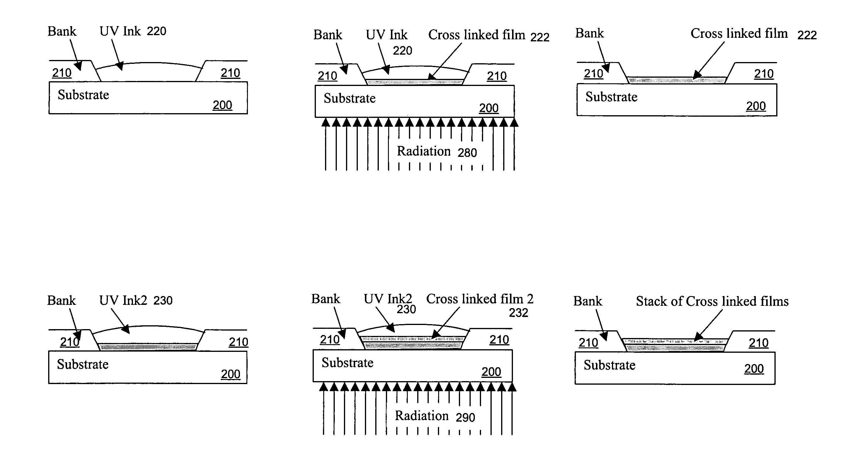
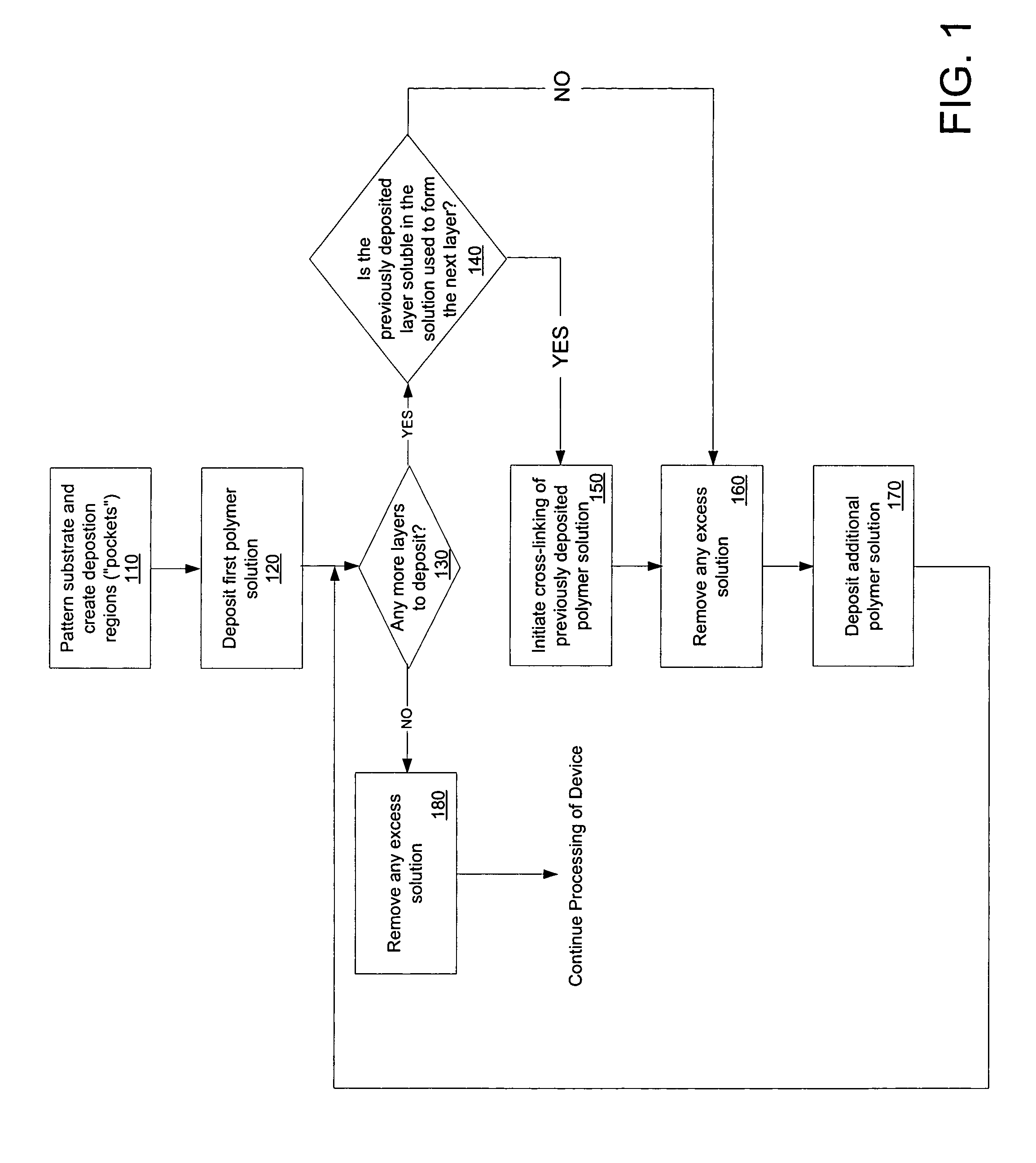
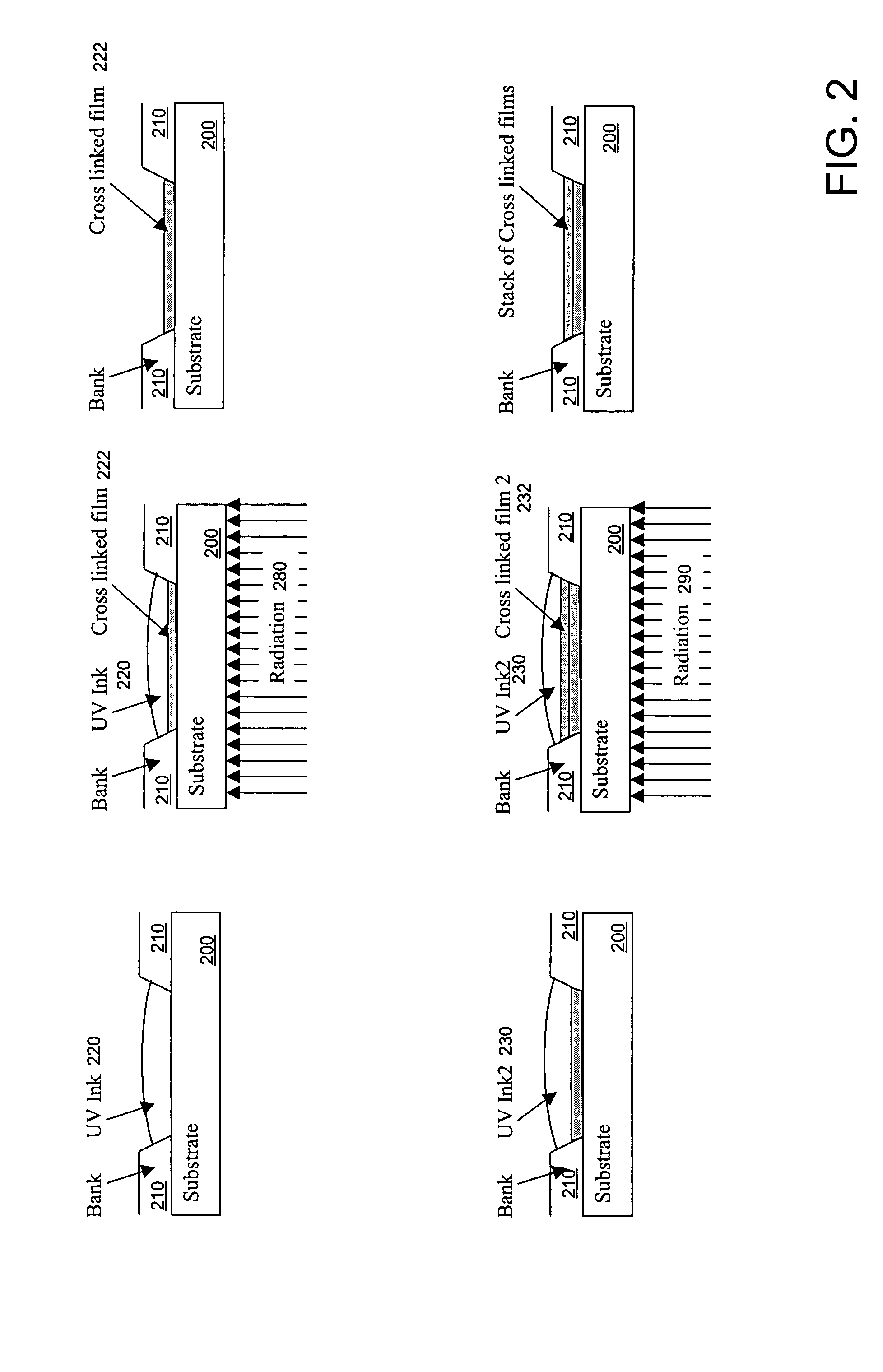
[0016] In accordance with the invention, a method for fabricating an organic electronic device is disclosed. The method consists primarily of 1) depositing a first organic solution by inkjet or other techniques, 2) cross-linking the deposited and dried (or partially dry or not dried organic film resulting therefrom), and then 3) depositing a second organic solution over the cross-linked film. This process can be extended to create hetero-structure devices containing three or more layers of film as well. Cross-linking is desirable if a previously deposited layer / film is soluble in the organic solution that is to follow. In such a case, cross-linking of the previously formed organic layer will cause it to become insoluble and thus, will prevent that layer from being degraded by another organic solution that is deposited over it.

[0017] In one embodiment of the invention, the organic solution used in fabricating the organic electronic device includes UV (ultra-violet) curable inks. UV ...


PUM

PropertyMeasurementUnit
work functionaaaaaaaaaa
thicknessaaaaaaaaaa
thicknessaaaaaaaaaa

Abstract

In accordance with the invention, a method for fabricating an organic electronic device is disclosed. The method consists primarily of 1) depositing a first organic solution by inkjet or other techniques, 2) cross-linking the deposited and dried (or partially dry or not dried organic film resulting therefrom, and then 3) depositing a second organic solution over the cross-linked film.

Description

CROSS-REFERENCE TO RELATED APPLICATIONS [0001] This application claims priority from a provisional patent application entitled “Method for Printing Organic Devices” filed on Jan. 16, 2004 bearing Ser. No. 60 / 537,414.BACKGROUND [0002] 1. Field of the Invention [0003] This invention relates generally to the art of thin film device processing and fabrication. More specifically, the invention relates to the fabrication of Organic Light Emitting Diode based displays and other devices. [0004] 2. Related Art [0005] Display and lighting systems based on LEDs (Light Emitting Diodes) have a variety of applications. Such display and lighting systems are designed by arranging a plurality of photo-electronic elements (“elements”) such as arrays of individual LEDs. LEDs that are based upon semiconductor technology have traditionally used inorganic materials, but recently, the organic LED (“OLED”) has come into vogue for certain applications. Examples of other elements / devices using organic materi...

Claims


Application Information

Patent Timeline
Patent Type & Authority Applications(United States)
IPC IPC(8): H01L51/00H01L51/30H01L51/40H01L51/56
CPCH01L51/0004H01L51/0036H01L51/0039H01L51/0038H01L51/0037H10K71/13H10K85/113H10K85/115H10K85/1135H10K85/114
Inventor GUPTA, RAHULINGLE, ANDREW
Owner OSRAM OPTO SEMICONDUCTORS GMBH
Why Eureka
Try Eureka