

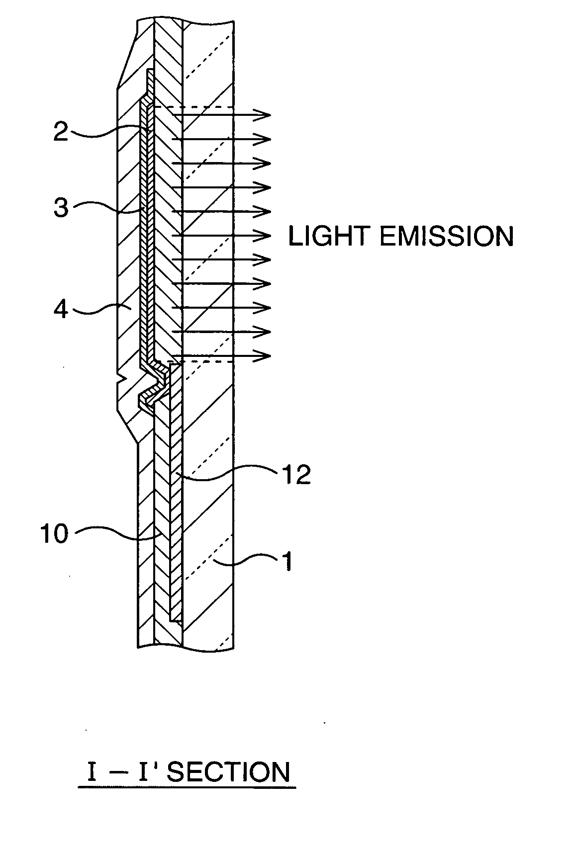
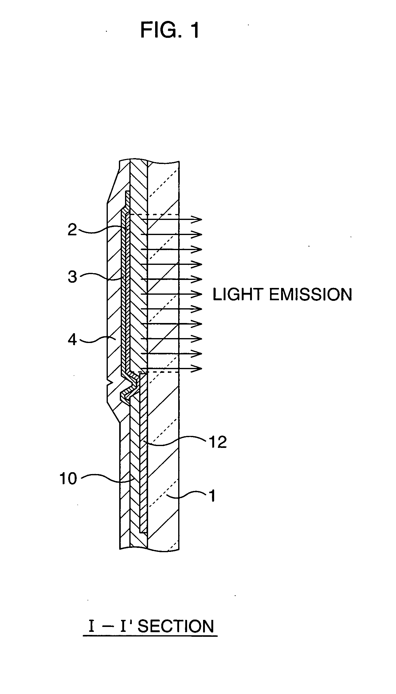
Display device and manufacturing method thereof
a technology of display device and manufacturing method, which is applied in the direction of identification means, instruments, discharge tube luminescnet screens, etc., can solve the problems of increasing power consumption, lowering the ratio of light emitting regions,
- Summary
- Abstract
- Description
- Claims
- Application Information
AI Technical Summary
Problems solved by technology
Method used
Image

Examples
embodiment
Modifications of Embodiment
[0045] Now, modifications of the embodiment will be described.
modification 1
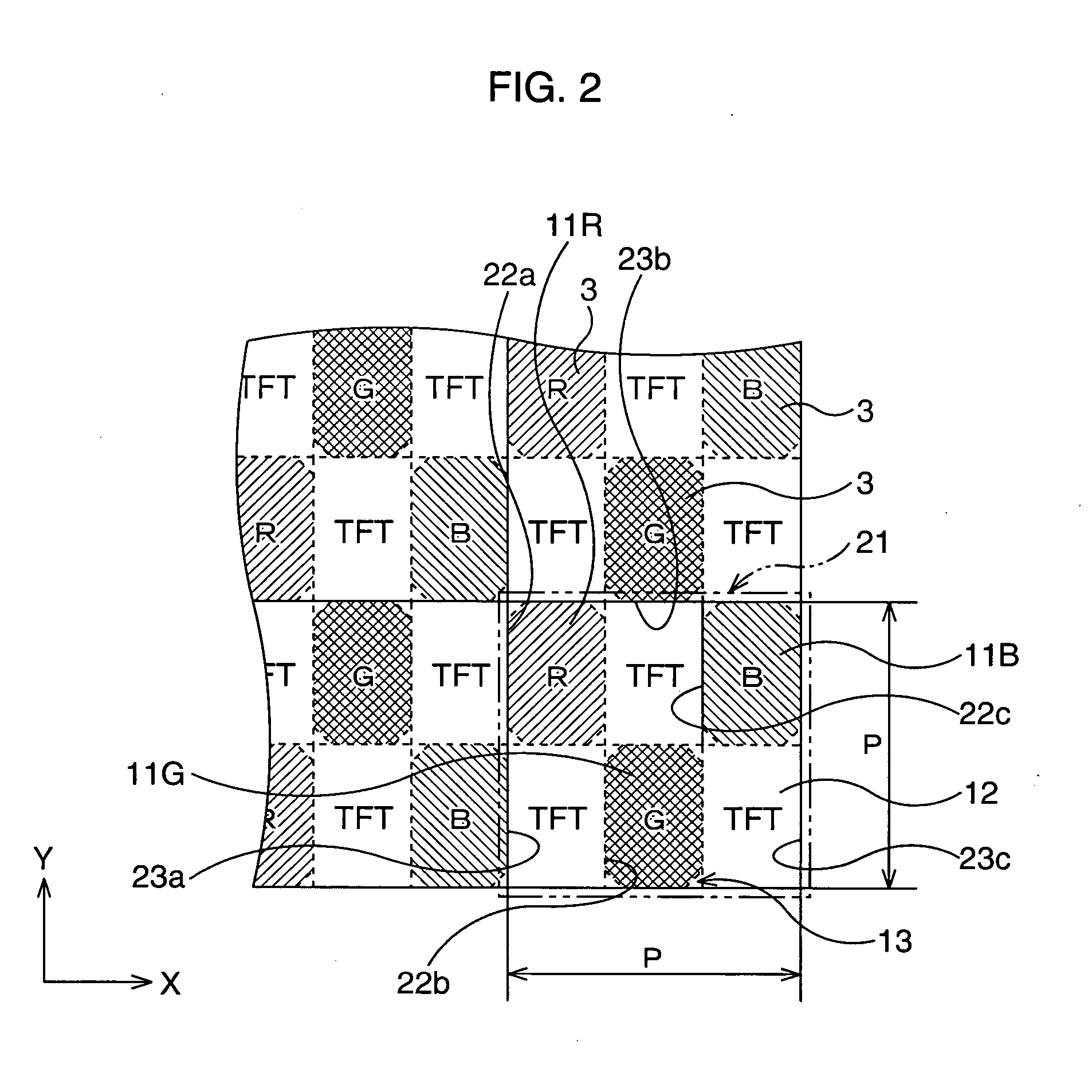
[0046]FIG. 7 is a schematic plan view of an organic EL light emitting layer, a main part of an organic EL display according to Modification 1, showing its surface as being enlarged.
[0047] In the organic EL display, the areas of the light emitting regions 11R, 11G, and 11B in the pixel 21 are each greater than the area of the TFT element 12. In this case, the registration margins necessary for discrete coloring into the three colors can be included in the segments of the TFT elements 12, so that the aperture ratio can be increased.
modification 2
[0048]FIG. 8 is a schematic plan view of an organic EL light emitting layer, a main part of an organic EL display according to Modification 2, showing its surface as being enlarged.
[0049] In this organic EL display, the areas of the light emitting regions 11R, 11G, and 11B in the pixel 21 are each smaller than the area of the TFT element 12. In this case, adjacent TFT elements 12 separate adjacent light emitting regions, and therefore there is no necessity for providing non-light emitting regions in association with the light emitting regions, so that the aperture ratio can be increased (in the shown example, the segments for the TFT elements 12 are in contact with each other).
PUM
 Abstract
Description
Claims
Application Information