Display device and driving method of the same

a technology of a display device and a driving method, which is applied in the direction of static indicating devices, instruments, material analysis, etc., can solve the problems of short circuit between both electrodes, thin thickness of an electroluminescent layer, and a likelihood of a similar defect to the aforementioned short circuit portion, so as to improve the deterioration of a light emitting element and improve image quality. , the effect of high reliability

Inactive Publication Date: 2005-07-28
SEMICON ENERGY LAB CO LTD
View PDF1 Cites 23 Cited by
  • Summary
  • Abstract
  • Description
  • Claims
  • Application Information

AI Technical Summary

Benefits of technology

[0008] In view of the aforementioned problems, the invention provides a display device, a driving method thereof, and an element substrate that a high image quality can be realized and a deterioration of a light emitting element can be improved.
[0009] In order to solve the aforementioned problems of a conventional technique, the invention employs a method to apply a reverse bias voltage to a light emitting element as one measure for improving reliability of the light emitting element. By applying a reverse bias voltage to a light emitting element, the light emitting element has a rectifying property as an electronic characteristic like a diode. Therefore, a current flows to a short-circuit portion although a reverse current does not flow. By flowing a current in a concentrated manner, the short-circuit portion can be burned out to be repaired.
[0018] According to the invention having the aforementioned structure, a display device that an effect due to variations in characteristics of transistors, in particular driving TFTs is suppressed and a high image quality is realized can be provided. Further, a display device that a deterioration of a light emitting element is improved and high reliability is realized can be provided.

Problems solved by technology

As an example of a defect of a light emitting element, there is a defect that a short-circuit occurs between both electrodes of the light emitting element.
This defect occurs when the both electrodes of the light emitting element contact each other without interposing an electroluminescent layer due to a defect in deposition of the electroluminescent layer caused by a dust, a projection and the like on a pixel electrode when forming the light emitting element.
As a defect of a light emitting element, there is another defect that the thickness of an electroluminescent layer becomes thin due to a dust in a deposition step of the light emitting element and the like.
In this case, the light emitting element emits light in initial stages, however, as a portion having thin film thickness has more stress than a periphery portion, a similar defect to the aforementioned short-circuited portion is likely to occur.
This defect is a progressive defect that comes up with an actual driving time, therefore, initial aging treatment may not be able to manage this in some cases.

Method used


Image

  • Display device and driving method of the same
  • Display device and driving method of the same
  • Display device and driving method of the same

Examples


embodiment 1

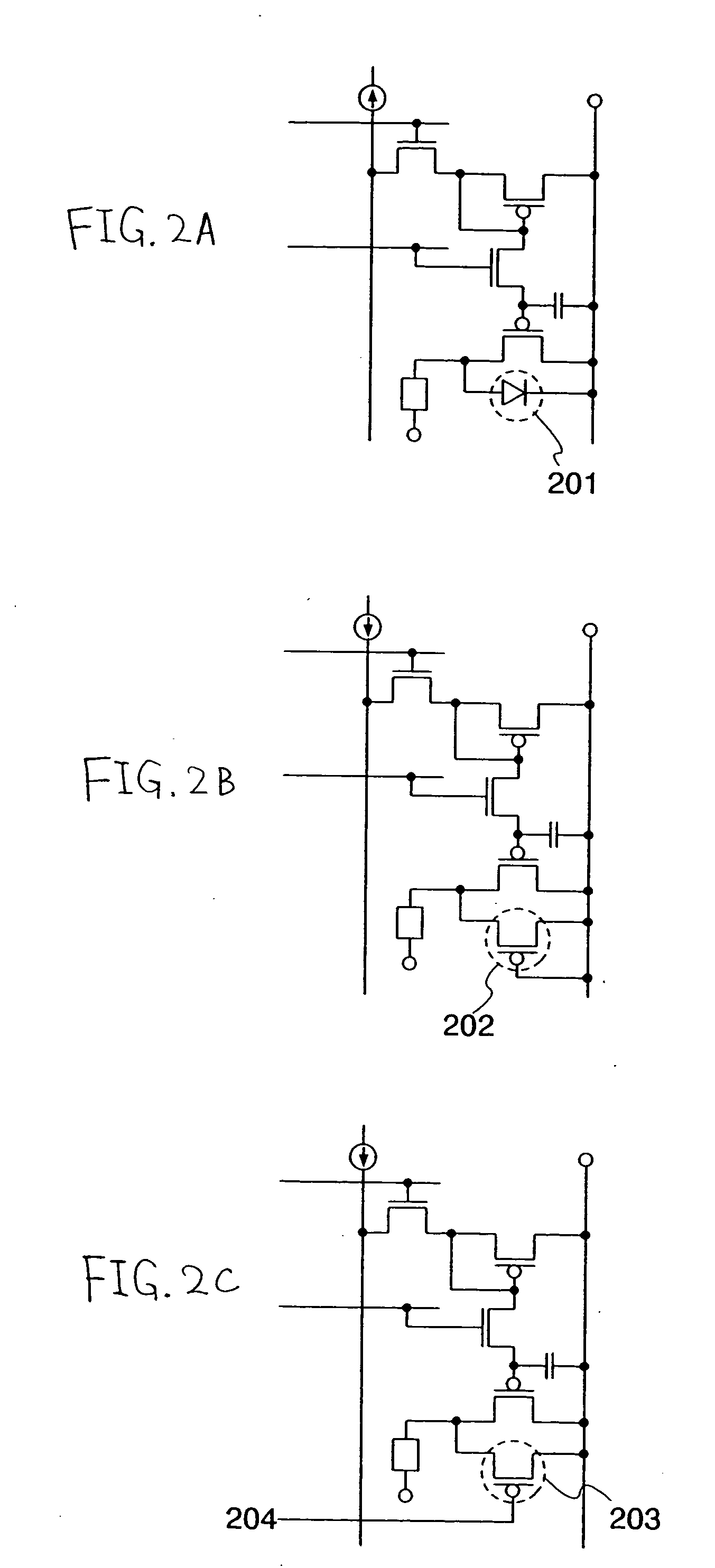
[0040] A structure of a light emitting element which is a component of the invention is described. The light emitting element corresponds to a lamination of a conductive layer, an electroluminescent layer, and a conductive layer provided on one surface of a substrate having an insulating surface such as glass, quartz, metal, organic substance and the like. The light emitting element may have any one of a lamination type of which electroluminescent layer is formed of a plurality of layers, a single layer type of which electroluminescent layer is formed of a single layer, and a hybrid type of which electroluminescent layer is formed of a plurality of layers but the boundary of them is not distinct. For the lamination structure of the light emitting element, there is a forward lamination structure that a conductive layer corresponding to an anode\an electroluminescent layer\a conductive layer corresponding to a cathode are laminated in this order from the bottom, and a reverse laminati...

embodiment 2

[0060] A panel mounted with a display region and a driver circuit, which is one mode of the display device of the invention is described with reference to FIGS. 5A and 5B. A display region 401 including a plurality of pixels each having a light emitting element, a source driver circuit 402, first and second gate driver circuits 403 and 404, a connecting terminal 415 and a connecting film 407 are provided on a substrate 405 (see FIG. 5A). The connecting terminal 415 is connected to the connecting film 407 through anisotropic conductive particles and the like. The connecting film 407 is connected to an IC chip.

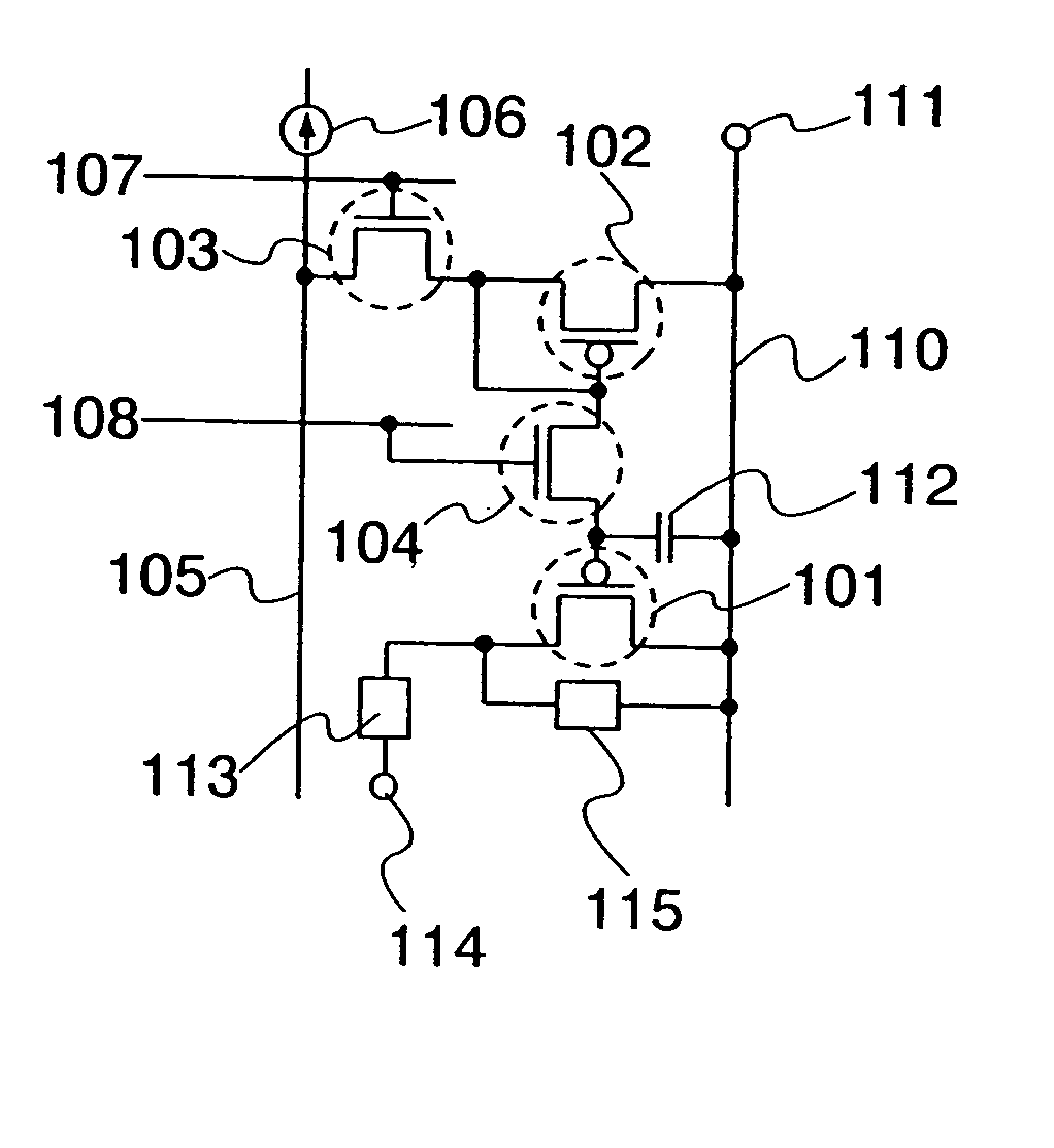
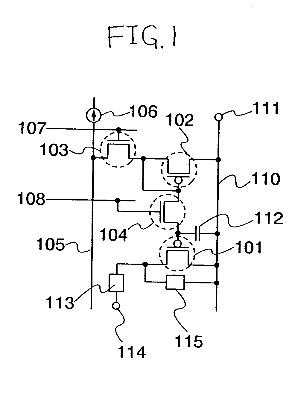
[0061]FIG. 5B shows a sectional diagram along A-A′ of the panel, including a driving TFT 101 provided in the display region 401 and a CMOS circuit 414 provided in the source driver circuit 402. In addition, a conductive layer 411, an electroluminescent layer 412 and a conductive layer 413 provided in the display region 401 are shown. The conductive layer 411 is connected to a s...

embodiment 3

[0072] Examples of electronic apparatuses provided with a display region including a light emitting element are, a television apparatus, a digital camera, a digital video camera, a portable telephone apparatus (a portable phone), a portable information terminal such as a PDA, a portable game machine, a monitor, a notebook personal computer, an audio reproducing apparatus such as a car audio set, an image reproducing apparatus provided with a recording medium such as a home game machine. Specific examples of these are described hereafter.

[0073]FIG. 7A illustrates a portable information terminal including a main body 9201, a display portion 9202 and the like. FIG. 7B illustrates a digital video camera including a display portion 9701, a main body 9702 and the like. FIG. 7C illustrates a portable terminal including a main body 9101, a display portion 9102 and the like. FIG. 7D illustrates a portable television apparatus including a main body 9301, a display portion 9302 and the like. ...


PUM


Abstract

The invention provides a display device, a driving method thereof, and an element substrate that a high image quality can be realized and a deterioration of a light emitting element can be improved. The invention includes a plurality of pixels arranged in matrix. Each of the plurality of pixels includes a light emitting element, a transistor, and an alternate current driving bypass element. The light emitting element and the transistor are connected in series and the alternate current driving bypass element and the transistor are connected in parallel.

Description

BACKGROUND OF THE INVENTION [0001] 1. Field of the Invention [0002] The present invention relates to a display device having a self-light emitting element and to a driving method thereof. The invention also relates to an element substrate having an element on an insulating surface. [0003] 2. Description of the Related Art [0004] In recent years, research and development of a display device having a self-light emitting element represented by an EL (Electro Luminescence) element is advanced, which is expected to be widely used by virtue of high image quality, wide viewing angle, and thin design, lightweight and the like without requiring a backlight. In general, a current value supplied to the EL element and luminance of the EL element are in proportion. Therefore, a pixel configuration which is different from an LCD of which luminance is controlled by a voltage value is suggested. For example, a pixel configuration that luminance is controlled by a current value is suggested (see Pat...

Claims


Application Information

Patent Timeline
Patent Type & Authority Applications(United States)
IPC IPC(8): G09G3/30G09G3/32H05B44/00
CPCG09G3/3241G09G2300/0426G09G2320/043G09G2300/0861G09G2310/0256G09G2300/0809
Inventor YAMAZAKI, SHUNPEI
Owner SEMICON ENERGY LAB CO LTD
Why Eureka
Try Eureka