
Optical interface assembly and method of formation

a technology of optical interfaces and assembly methods, applied in the field of optical communication systems, can solve the problems of no known method of directly coupling light from an incoming fiber, the inability of copper interconnect technology to scale to the bandwidth requirements of processing units, and the inability to provide a direct interface between the two

Active Publication Date: 2005-07-28
ROHM & HAAS ELECTRONICS MATERIALS LLC
View PDF19 Cites 33 Cited by
  • Summary
  • Abstract
  • Description
  • Claims
  • Application Information

AI Technical Summary

Benefits of technology

[0011] Accordingly, it would be desirable to be able to conveniently and reliably couple/decouple light fr...

Problems solved by technology

With the dramatic increase in processor speed over the last several years and the anticipation that this trend will continue, the copper interconnect technology will be unable to scale to the bandwidth requirements of the processing units.
Currently, there are no known available methods for directly coupling light from an incoming fiber to embedded waveguides formed within a printed wiring board (PWB) substrate.
However, the Morse disclosure still does not provide a direct interface between, for example, a fiber optic connector and optical waveguides formed within a printed wiring board.

Method used


Image

  • Optical interface assembly and method of formation
  • Optical interface assembly and method of formation
  • Optical interface assembly and method of formation

Examples


Embodiment Construction

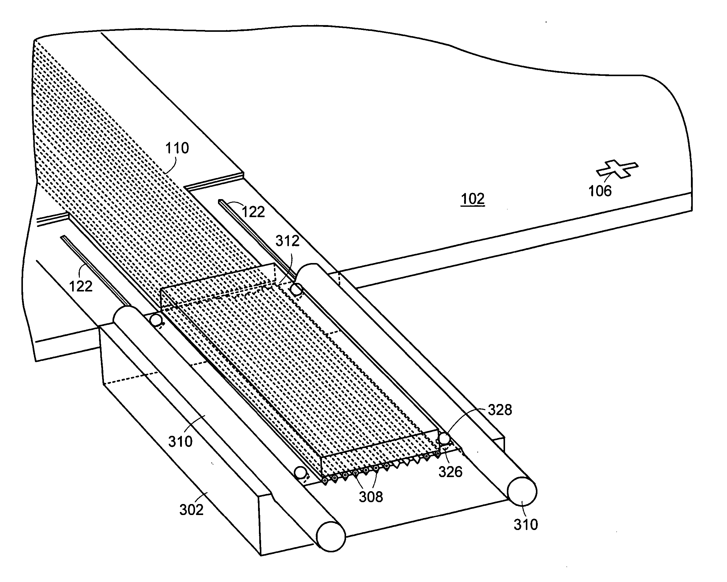
[0019] Disclosed herein is a method and structure for coupling optical fibers with embedded waveguides formed within an electronic substrate. Briefly stated, an optical interface assembly includes a first portion and a second portion, wherein the first portion is configured to house a plurality of optical fibers therein and for mating engagement with an optical fiber connector at a first end thereof. The optical fiber connector can be, for example, an MT connector and the like. As used hereinafter, the term “electronic substrate” may describe structures such as, for example, printed wiring board substrates, semiconductor substrates, glass substrates, mylar substrates, and the like. For purposes of description, the term “printed wiring board” (PWB) or “PWB substrate” is also used interchangeably hereinafter with the term “electronic substrate.”

[0020] As set forth in further detail later, a mating engagement between various constituent components is described in terms of one or more t...


PUM


Abstract

Optical interface assemblies are provided. The optical interface assemblies include a first portion having a plurality of optical waveguides. The first portion is configured for mating engagement with an optical fiber connector. A second portion is mated to the first portion. The second portion is configured for mating engagement with an electronic substrate that includes an embedded waveguide assembly. The first and second portions are further configured so as to align the plurality of optical waveguides, at a first end of the first portion, with a plurality of corresponding waveguide cores of the embedded waveguide assembly. The first and second portions are further configured so as to align the plurality of optical waveguides, at a second end of the first portion, with a plurality of corresponding optical fibers in the optical fiber connector. Also provided are electronic assemblies and methods for coupling optical fibers with electronic substrate embedded waveguides.

Description

CROSS-REFERENCE TO RELATED APPLICATIONS [0001] This application claims the benefit under 35 U.S.C. §119(e) of U.S. Provisional Application No. 60 / 532,020, filed Dec. 22, 2003, the entire contents of which are incorporated herein by reference.BACKGROUND [0002] The present invention relates generally to optical communication systems, and, more particularly to a method and structure for coupling optical fibers with printed wiring board embedded waveguides. [0003] There are many well-recognized benefits of using optical fiber to replace copper wiring for printed circuit boards (PCBs) in computer and networking equipment. Such potential benefits include increased bandwidth and data rate, overcoming bottlenecks in the processing architecture, immunity to electromagnetic interference and reductions in radiated noise from the system, reduced latency by elimination of optical / electrical (O / E) conversions, more dense packaging at lower cost per pin, and enablement of new processor interconnec...

Claims


Application Information

Patent Timeline
IPC IPC(8): G02B6/122G02B6/30G02B6/24G02B6/36G02B6/38G02B6/42H05K1/02
CPCG02B6/1221G02B6/30G02B6/3636G02B6/3652G02B6/3688G02B6/4249G02B6/3696G02B6/3885G02B6/421G02B6/423G02B6/3692E01C9/005A01G13/0293A01G13/0237
Inventor MOYNIHAN, MATTHEW L.SICARD, BRUNO M.COLANGELO, CARL J.CAHALEN, JOHN P.AMOS, BRIAN D.HORGAN, KEVIN S.FISHER, JOHN J.SHERRER, DAVID W.
Owner ROHM & HAAS ELECTRONICS MATERIALS LLC
Features
  • Generate Ideas
  • Intellectual Property
  • Life Sciences
  • Materials
  • Tech Scout
  • Unparalleled Data Quality
  • Higher Quality Content
  • 60% Fewer Hallucinations
Learn More