Array substrate and display apparatus and method for manufacturing display apparatus

a technology of array substrate and display apparatus, which is applied in the direction of identification means, instruments, refuse gathering, etc., can solve the problems of inability to analyze inability to achieve analysis of defects due to defective output voltage of drive circuit or the like, and inability to perform defect analysis. , to achieve the effect of preventing the occurrence of electrostatic destruction

Inactive Publication Date: 2005-08-04
MITSUBISHI ELECTRIC CORP +1
View PDF2 Cites 4 Cited by
  • Summary
  • Abstract
  • Description
  • Claims
  • Application Information

AI Technical Summary

Benefits of technology

[0010] The invention can provide an array substrate and a display apparatus, each of which is adapted so that the defect analysis can be performed by monitoring electric potential supplied to a signal line after a completed product is obtained, and that occurrence of electrostatic destruction can be prevented, and also can provide a method for manufacturing the display apparatus.

Problems solved by technology

However, the former conventional display apparatus has problems that although the state of the defects can be judged according to the display condition by using the monitoring electrodes, the condition of electric potential actually applied to signal lines cannot be monitored, and that analysis of defects due to a defective output voltage of a drive circuit or the like cannot be achieved.
Thus, it is impossible to perform the defect analysis by observing of a voltage applied to the actual signal line and by monitoring electric potential applied to each of the signal lines after the product is actually obtained.

Method used


Image

  • Array substrate and display apparatus and method for manufacturing display apparatus
  • Array substrate and display apparatus and method for manufacturing display apparatus
  • Array substrate and display apparatus and method for manufacturing display apparatus

Examples


first embodiment

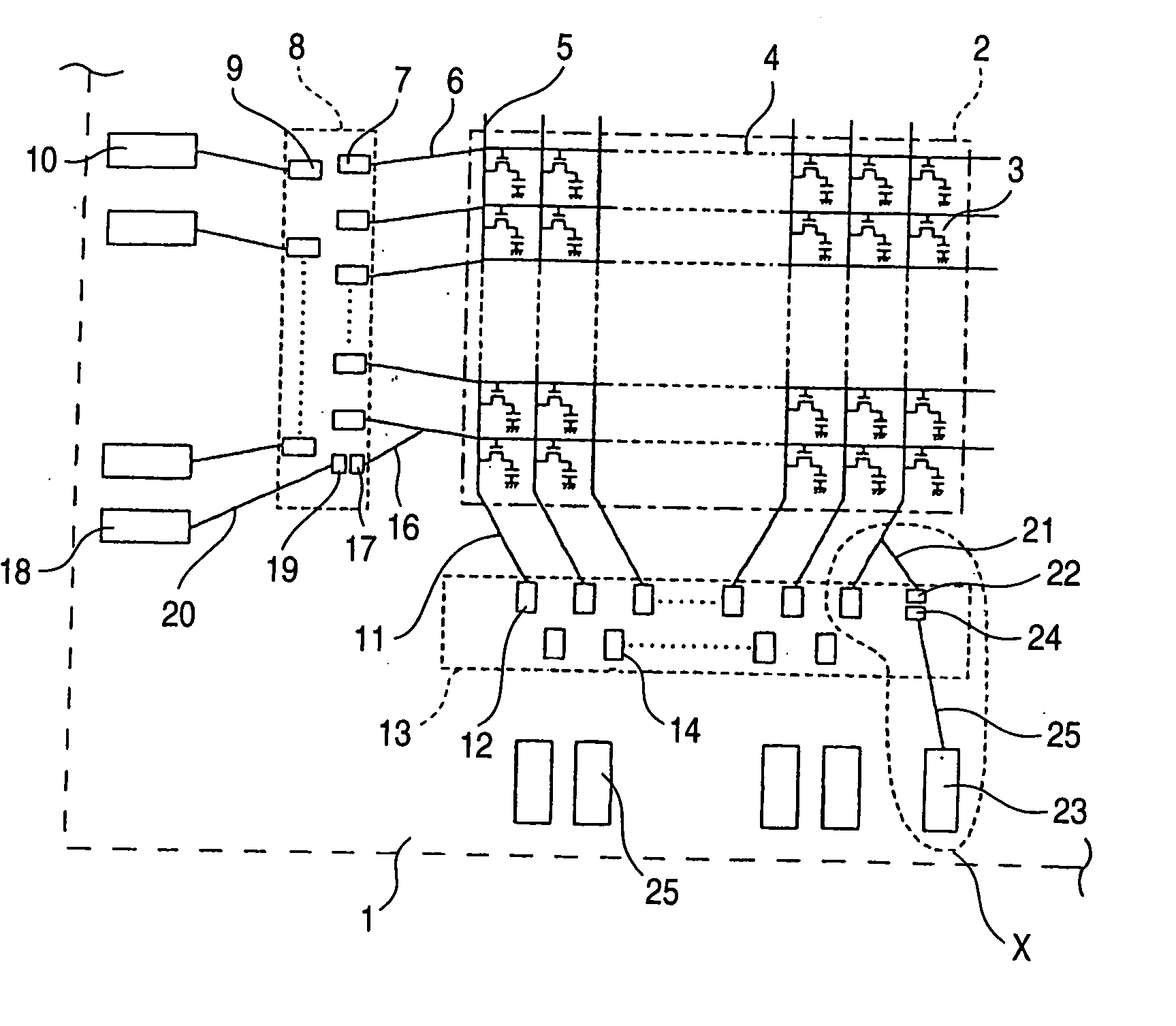
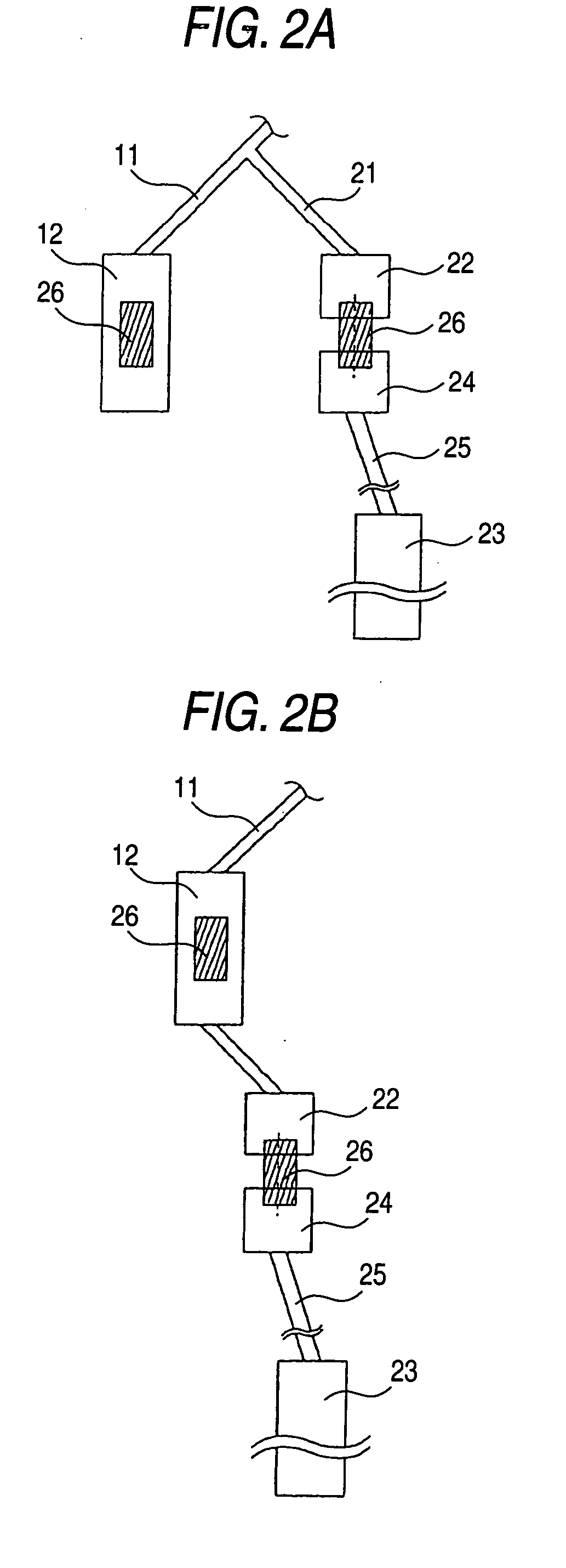
[0018] A first embodiment of the invention is described hereinbelow by referring to FIGS. 1 to 3. FIG. 1 shows an equivalent circuit diagram of a display apparatus of the first embodiment of the invention. FIGS. 2A and 2B are enlarged diagrams of a video-signal-line-side monitoring terminal portion X shown in FIG. 1. FIG. 3 is a cross-sectional diagram taken on line A-A shown in each of FIGS. 2A and 2B.

[0019] As shown in FIG. 1, scanning lines 4, which are connected to the gates of thin film transistors 3 respectively provided in pixels constituting a display area 2 and supply scanning signals thereto, and video signal lines 5, which are connected to the sources of the thin film transistors 3 and supply video signals thereto, are disposed on an insulating substrate 1. The scanning lines 4 are drawn to the outside of the display area 2 through scanning line lead-out wires 6 and connected to signal line terminals 7 thereof. A scanning line driving circuit 8 is mounted on the insulati...

second embodiment

[0029] A second embodiment of the invention is described hereinbelow by referring to FIGS. 4 and 5A to 5C. FIG. 4 shows an equivalent circuit diagram illustrating a display apparatus according to the second embodiment of the invention. FIG. 5A shows a schematic diagram illustrating a video signal line driving circuit in an enlarged view of a video-signal-line-side monitoring terminal portion Y shown in FIG. 4. FIGS. 5B and 5(c) show schematic diagrams each illustrating a pattern formed on an insulating substrate in an enlarged view of the video-signal-line-side monitoring terminal portion Y.

[0030] In FIG. 4, constituent parts, which are the same as those shown in FIGS. 1 to 3, are designated by the same reference characters as those used in FIGS. 1 to 3. Thus, the differences between these embodiments are described hereinbelow. As shown in FIG. 4, for example, the signal line terminal 7 associated with the scanning line, which is connected to one of endmost wires of the group of sc...

third embodiment

[0038] A third embodiment of the invention is described herein below with reference to FIG. 6. FIG. 6 shows an equivalent circuit diagram illustrating a display apparatus according to the third embodiment of the invention.

[0039] In FIG. 6, constituent parts, which are the same as those shown in FIGS. 1 to 5C, are designated by the same reference characters as those used in FIGS. 1 to 5C. Thus, the differences among the embodiments are described hereinbelow. As shown in FIG. 6, an inspection circuit 44 is formed at the video-signal-line-side part on the insulating substrate. Inspection circuit wires 45 for inputting various signals to the inspection circuit 44 are connected to inspection terminals formed in parallel with the video-signal-line-side external terminals 15. Incidentally, similarly to the first and second embodiments, one of the inspection circuit wires 45 has an inspection circuit wire connecting portion 47. Incidentally, the inspection circuit is formed by being the si...


PUM

PropertyMeasurementUnit
conductiveaaaaaaaaaa
electrical potentialaaaaaaaaaa
electric potentialaaaaaaaaaa

Abstract

An array substrate according to the invention includes an external terminal formed in the vicinity of an end portion of an insulating substrate so as to supply electric potential from the exterior to a driving circuit, a signal line monitoring terminal formed in parallel with the external terminal, a signal line branch terminal formed in such a way as to be connected to a signal line or to a signal line terminal, and an internal terminal associated with the signal line monitoring terminal, which is connected to the signal line monitoring terminal and connectable to a signal line branch terminal by an electrically conductive material and a bump of the driving circuit.

Description

BACKGROUND OF THE INVENTION [0001] 1. Field of the Invention [0002] The present invention relates to an array substrate and a display apparatus, each of which is adapted so that the monitoring of electric potential supplied to a signal line can be observed (or monitored) and that occurrence of electrostatic destruction can be prevented, and to a method for manufacturing the display apparatus. [0003] 2. Description of the Related Art [0004] In a conventional display apparatus, for example, when various defects caused in a completed product are analyzed, first, monitoring electrodes are individually connected to scanning-signal wires and / or video signal wires outside a display area. Then, defect analysis is performed according to the conditions of pixels associated with each of the monitoring electrodes and the display conditions of those disposed within a display area in a driven state (see, for instance, JP-A-9-264917). [0005] Further, another conventional display apparatus has an i...

Claims


Application Information

Patent Timeline
Patent Type & Authority Applications(United States)
IPC IPC(8): G01R31/02G01R31/00G02F1/13G02F1/1345G09F9/00G09G3/00G09G5/00
CPCG09G3/006B65D25/325B65F1/06B65F1/1415
Inventor NAKAYAMA, AKIOIIDA, SHUICHI
Owner MITSUBISHI ELECTRIC CORP
Why Eureka
Try Eureka