Apparatus and method for clamping reset voltage in image sensor

a technology of image sensor and reset voltage, which is applied in the field of image sensor, can solve the problems of ccd with a more complicated fabrication process, a large number of mask steps, and a more complicated driver and power consumption, and achieve the effect of accurately accounting for fabrication

Inactive Publication Date: 2005-08-04
SAMSUNG ELECTRONICS CO LTD
View PDF5 Cites 24 Cited by
  • Summary
  • Abstract
  • Description
  • Claims
  • Application Information

AI Technical Summary

Benefits of technology

[0018] Accordingly, the present invention has more flexibility for clamping a reset voltage within an image sensor.
[0025] In this manner, the reset voltage is clamped separately for each column of the array of pixels in the image sensor for more accurately accounting for fabrication variations along such columns. In addition, a fixed clamping voltage is not used across the whole array of pixels for more flexibly clamping the reset voltage across the array of pixels.

Problems solved by technology

The CCD has a more complicated fabrication process with a relatively large number of mask steps.
In addition, the CCD has more complicated drivers and higher power consumption.
Furthermore, the CCD is typically not fabricated as a single chip with a separate chip being fabricated for a signal processor from the chip for the CCD array.
For example, when excessive light is present during resetting of the photodiode, the first output voltage V1 may be too low.
In that case, image distortion results even when correlated double sampling is used in the CMOS image sensor.
Thus, the reset voltage may not be accurately controlled since the reset voltage may vary across the different locations of the array of pixels from fabrication variations.

Method used


Image

  • Apparatus and method for clamping reset voltage in image sensor
  • Apparatus and method for clamping reset voltage in image sensor
  • Apparatus and method for clamping reset voltage in image sensor

Examples


Embodiment Construction

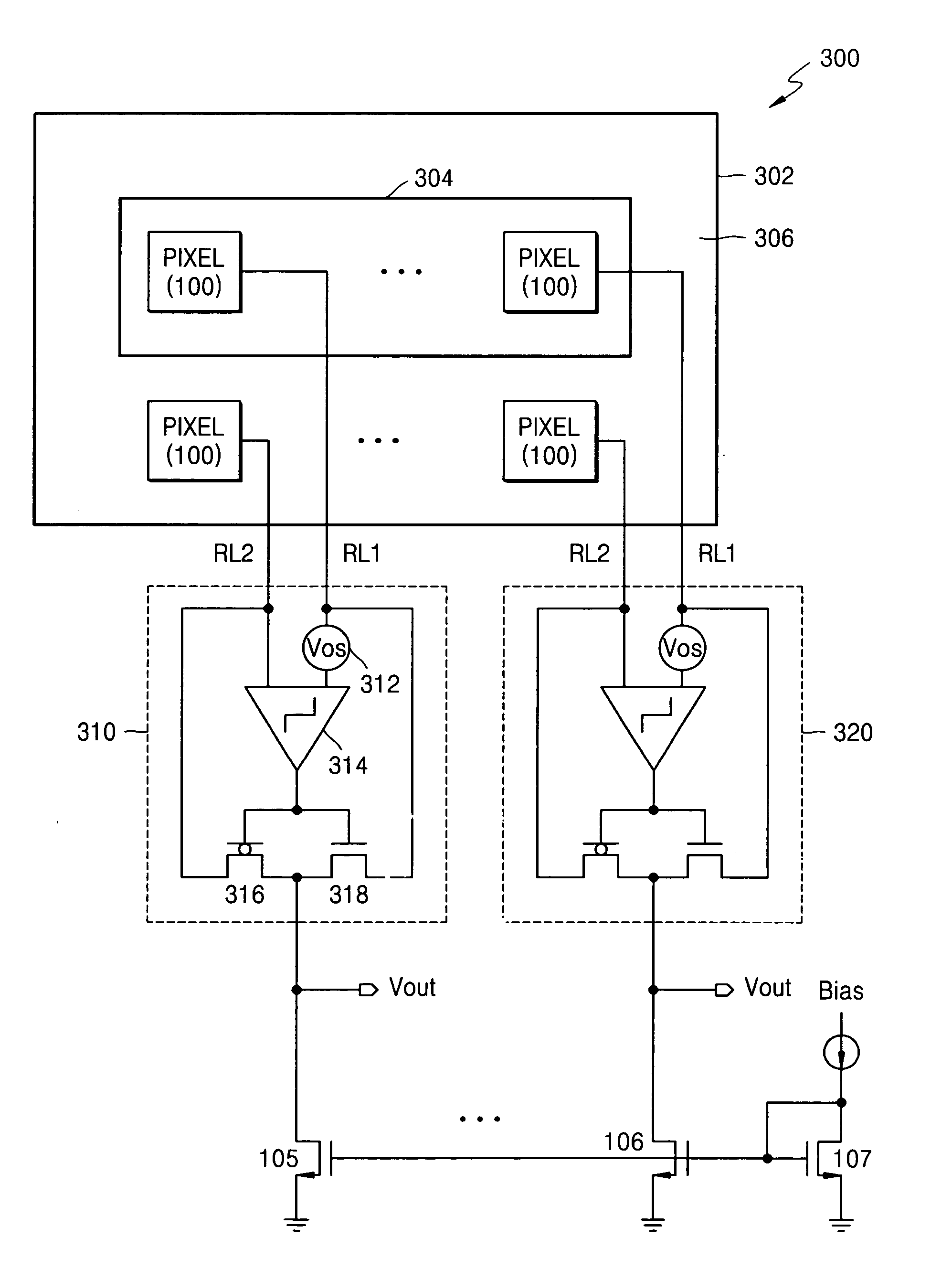
[0032]FIG. 3 shows a schematic diagram of an apparatus for clamping a reset voltage within a CMOS image sensor according to an embodiment of the present invention. Referring to FIG. 3, a CMOS image sensor 300 includes an array 302 of pixels 100 arranged in rows and columns. The array 302 includes an active region 304 that is a portion of the array 302 and includes an optical black (OB) region 306 surrounding the active region 304.

[0033] A pixel 100 located within the active region 304 is hereafter referred to as an active pixel, and a pixel 100 located within the OB region 306 is hereafter referred to as an optical black pixel. The active pixels within the active region 304 are exposed to light, whereas the optical black pixels within the OB region 306 are shielded from light.

[0034] Each column of the array 302 has a respective active pixel in the active region 304 and a respective optical black pixel in the OB region 306. The respective active pixel generates a respective first r...


PUM


Abstract

For clamping a reset voltage within an image sensor, an active pixel generates a first reset voltage, and an optical black pixel generates a second reset voltage. In addition, a reset voltage selector selects one of the first and second reset voltages as a selected reset voltage. Such a selected reset voltage is generated separately for each column of the array of pixels in the image sensor for more accurately and flexibly accounting for fabrication variations.

Description

BACKGROUND OF THE INVENTION [0001] This application claims priority to Korean Patent Application No. 2004-7214, filed on Feb. 4, 2004, in the Korean Intellectual Property Office, the disclosure of which is incorporated herein in its entirety by reference. [0002] 1. Field of the Invention [0003] The present invention relates generally to image sensors, and more particularly, to clamping of reset voltage in an image sensor, such as a CMOS image sensor that performs correlated double sampling. [0004] 2. Description of the Related Art [0005] An image sensor is a semiconductor device that converts an optical image into electrical signals. Examples of an image sensor include a charge coupled device (CCD) and a CMOS (complementary metal oxide semiconductor) image sensor. The CCD includes densely arranged MOS capacitors with charge carriers stored in the capacitors and transferred among the capacitors. [0006] A CMOS image sensor includes pixels with each pixel including a photodiode and MOS...

Claims


Application Information

Patent Timeline
Patent Type & Authority Applications(United States)
IPC IPC(8): H04N5/16H04N5/335H04N5/357H04N5/363H04N5/374H04N5/378
CPCH04N5/363H04N5/3575H04N25/616H04N25/65B60J3/0239
Inventor HAN, JUNE-SOO
Owner SAMSUNG ELECTRONICS CO LTD
Why Eureka
Try Eureka