Semiconductor memory device using tapered arrangement of local input and output sense amplifiers

a memory device and tapered arrangement technology, applied in the direction of information storage, static storage, digital storage, etc., can solve the problems of increased power consumption of the amplifier and inadequacies of the conventional arrangement of the lio sense amplifier, and achieve the effect of increasing the power consumption of the amplifier and extending the driving rang

Inactive Publication Date: 2005-08-04
SAMSUNG ELECTRONICS CO LTD
View PDF5 Cites 5 Cited by
  • Summary
  • Abstract
  • Description
  • Claims
  • Application Information

AI Technical Summary

Benefits of technology

[0011] In order to compensate for such time differences, it is possible to design the driving capabilities of the LIO sense amplifiers by considering the longest one of the cell data transfer paths. However, the chip size corresponding to an amplifier, particularly a transistor for an output driving part, must be large to implement an amplifier with a large driving capability. Also, power consumption of the amplifier is increased.

Problems solved by technology

However, the chip size corresponding to an amplifier, particularly a transistor for an output driving part, must be large to implement an amplifier with a large driving capability.
Also, power consumption of the amplifier is increased.
Therefore, the conventional LIO sense amplifier arrangement is not appropriate for the current technical trend requiring minimization and lower power consumption.

Method used


Image

  • Semiconductor memory device using tapered arrangement of local input and output sense amplifiers
  • Semiconductor memory device using tapered arrangement of local input and output sense amplifiers
  • Semiconductor memory device using tapered arrangement of local input and output sense amplifiers

Examples


Embodiment Construction

[0027] In the description to follow, the same or similar elements are indicated in the drawings by the same reference numerals.

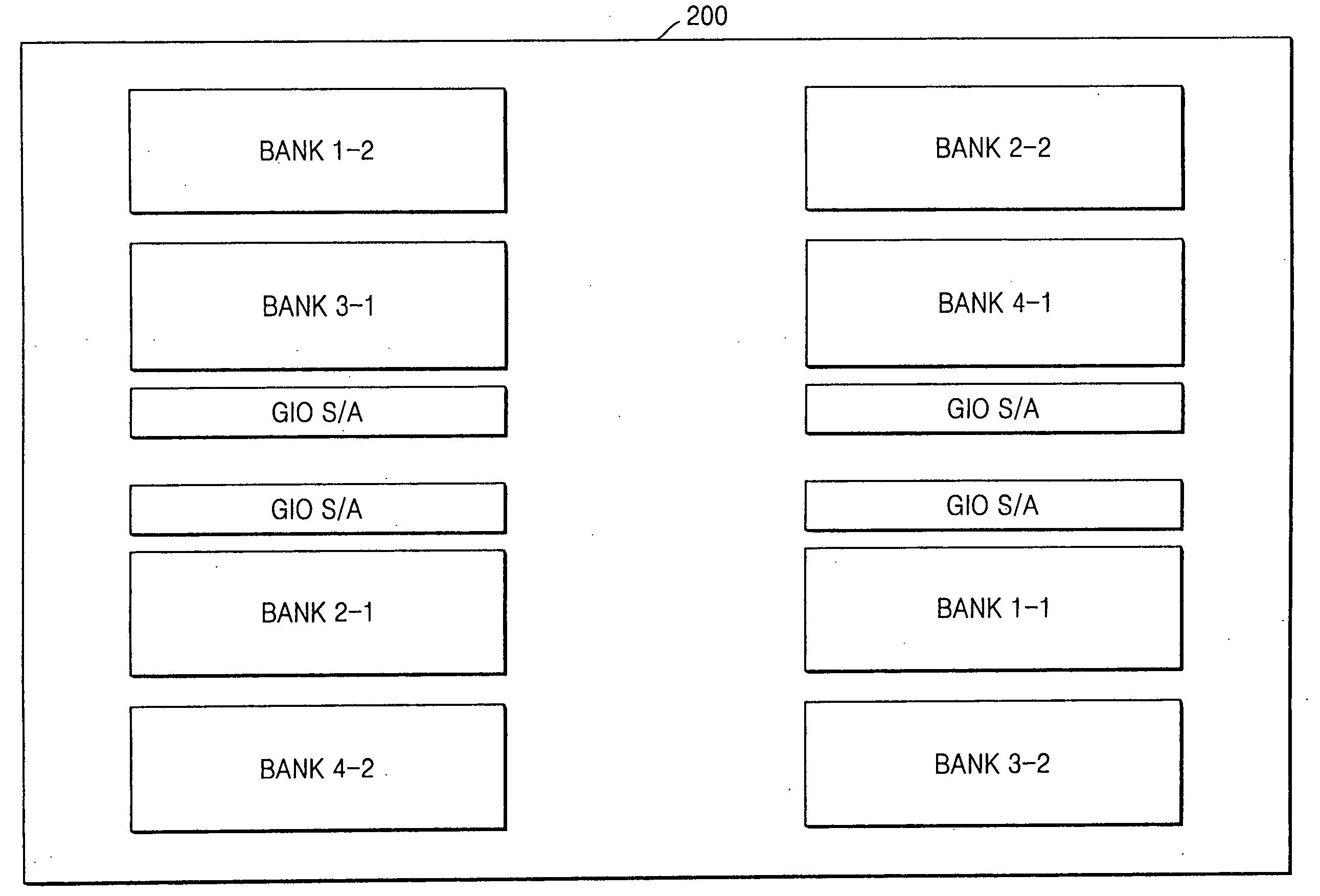
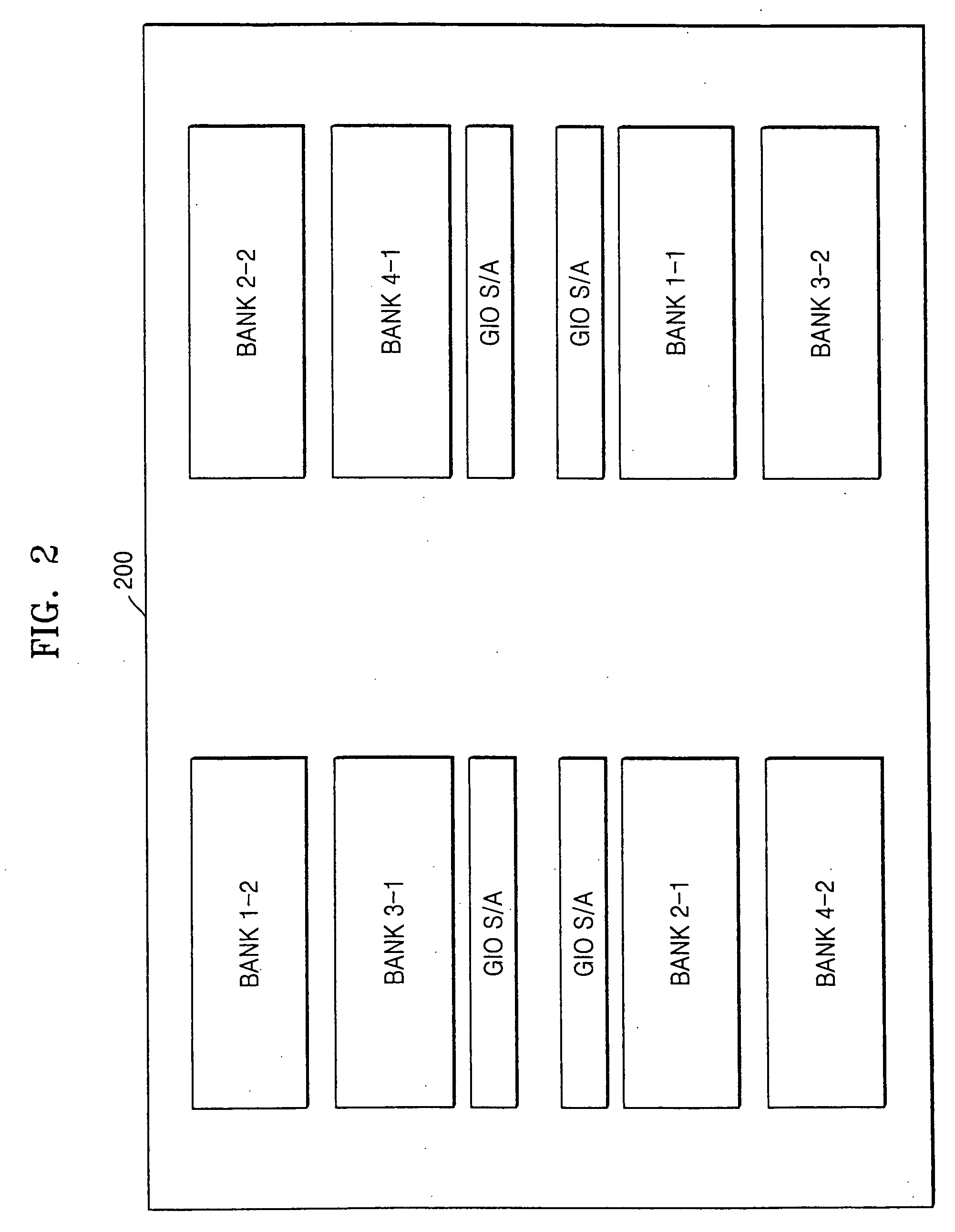
[0028]FIG. 2 shows a block diagram of a semiconductor memory device 200 comprising four banks, 1 through 4. Furthermore, each bank comprises a pair of sub-banks.

[0029] The first bank 1 comprises a first sub-bank BANK 1-1 arranged nearer to the global input & output (GIO) sense amplifier S / A, and a second sub-bank BANK 1-2 arranged farther away from the GIO sense amplifier S / A.

[0030] Similarly, the second bank 2 comprises a first sub-bank BANK 2-1 arranged nearer to the GIO sense amplifier S / A and a second sub-bank BANK 2-2 arranged farther away from the GIO sense amplifier S / A.

[0031] Similarly, the third bank 3 comprises a first sub-bank BANK 3-1 arranged nearer to the GIO sense amplifier S / A and a second sub-bank BANK 3-2 arranged farther away from the GIO sense amplifier S / A.

[0032] Similarly, the fourth bank 4 comprises a first sub-bank BANK 4-1 arran...


PUM


Abstract

A semiconductor memory device optimizes current consumption by using proper sub-bank arrangement and at least two different kinds of LIO sense amplifiers having different driving capabilities. The driving capabilities of the LIO sense amplifiers are controlled in a tapered manner depending on whether a corresponding sub-bank of the LIO sense amplifier is arranged nearer to, or farther away from, its corresponding GIO sense amplifier. In other words, the farther that a sub-bank of an LIO sense amplifier is away from its corresponding GIO sense amplifier, the greater its driving capability.

Description

CROSS REFERENCES TO RELATED APPLICATIONS [0001] This application claims priority under 35 U.S.C. § 119 from Korean Patent Application No. 04-5648, filed on Jan. 29, 2004, the contents of which are hereby incorporated by reference in their entirety for all purposes as if fully set forth herein. BACKGROUND AND SUMMARY [0002] 1. Technical Field. [0003] The present invention relates to a semiconductor memory device, and more particularly, to a memory architecture using a tapered arrangement of local input & output (LIO) sense amplifiers. [0004] 2. Description of the Related Art. [0005]FIG. 1 shows a block diagram of a dynamic random access memory (DRAM) core of a conventional semiconductor memory device. [0006] From FIG. 1, one can recognize paths for reading cell data from the banks 0-2 and 2-1 in a conventional DRAM core 100 comprising a plurality of banks. [0007] In order to read out one or a plurality of data from the memory cells of the semiconductor memory device, the data stored ...

Claims


Application Information

Patent Timeline
Patent Type & Authority Applications(United States)
IPC IPC(8): G11C7/06G11C5/02G11C7/02G11C11/4097
CPCG11C11/4097G11C5/025G11C7/06G11C11/4091
Inventor KIM, YOUN-CHEUL
Owner SAMSUNG ELECTRONICS CO LTD
Why Eureka
Try Eureka