

Method for identifying bead location information
- Summary
- Abstract
- Description
- Claims
- Application Information
AI Technical Summary
Benefits of technology
Problems solved by technology
Method used
Image

Examples
Embodiment Construction
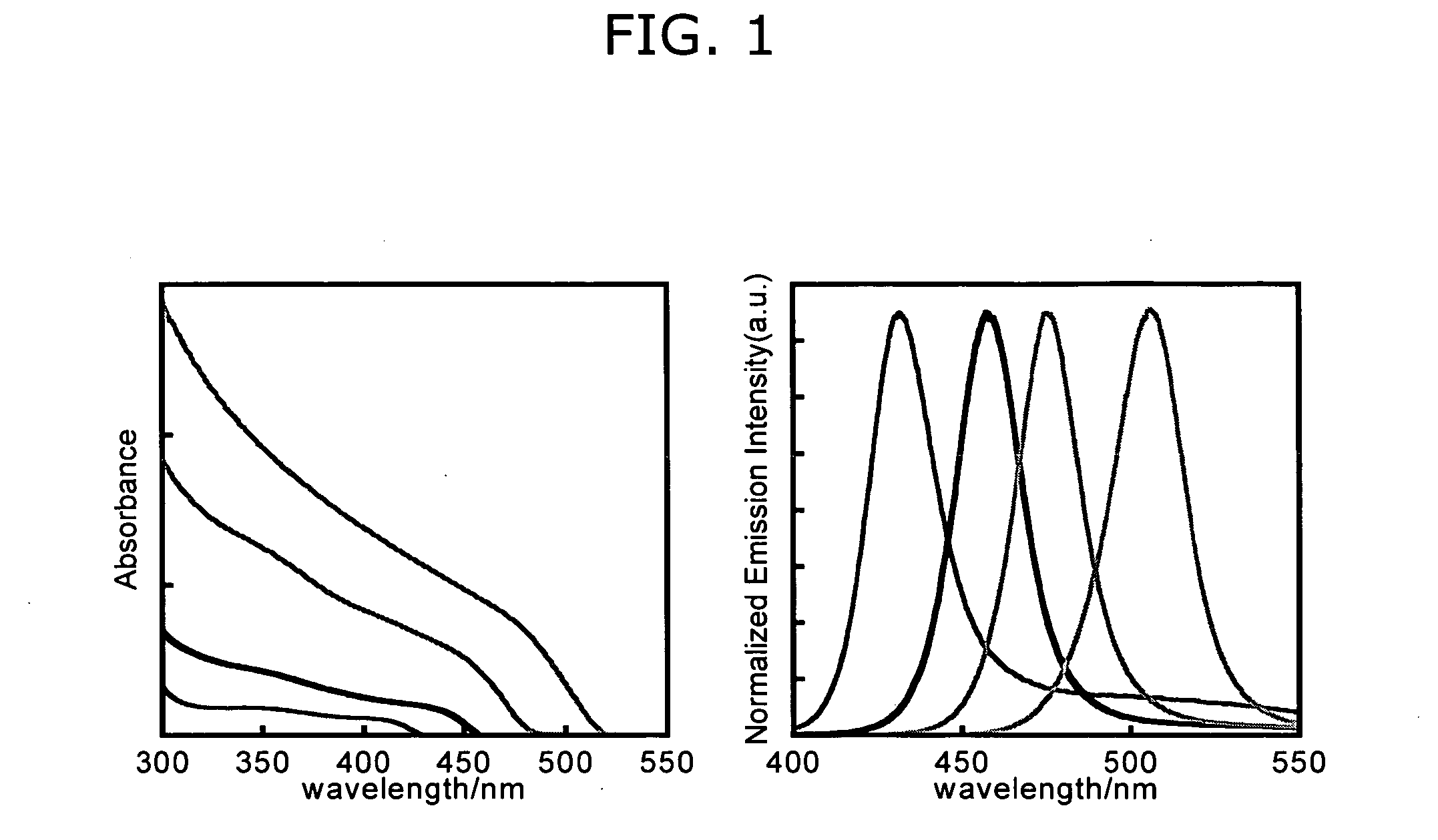
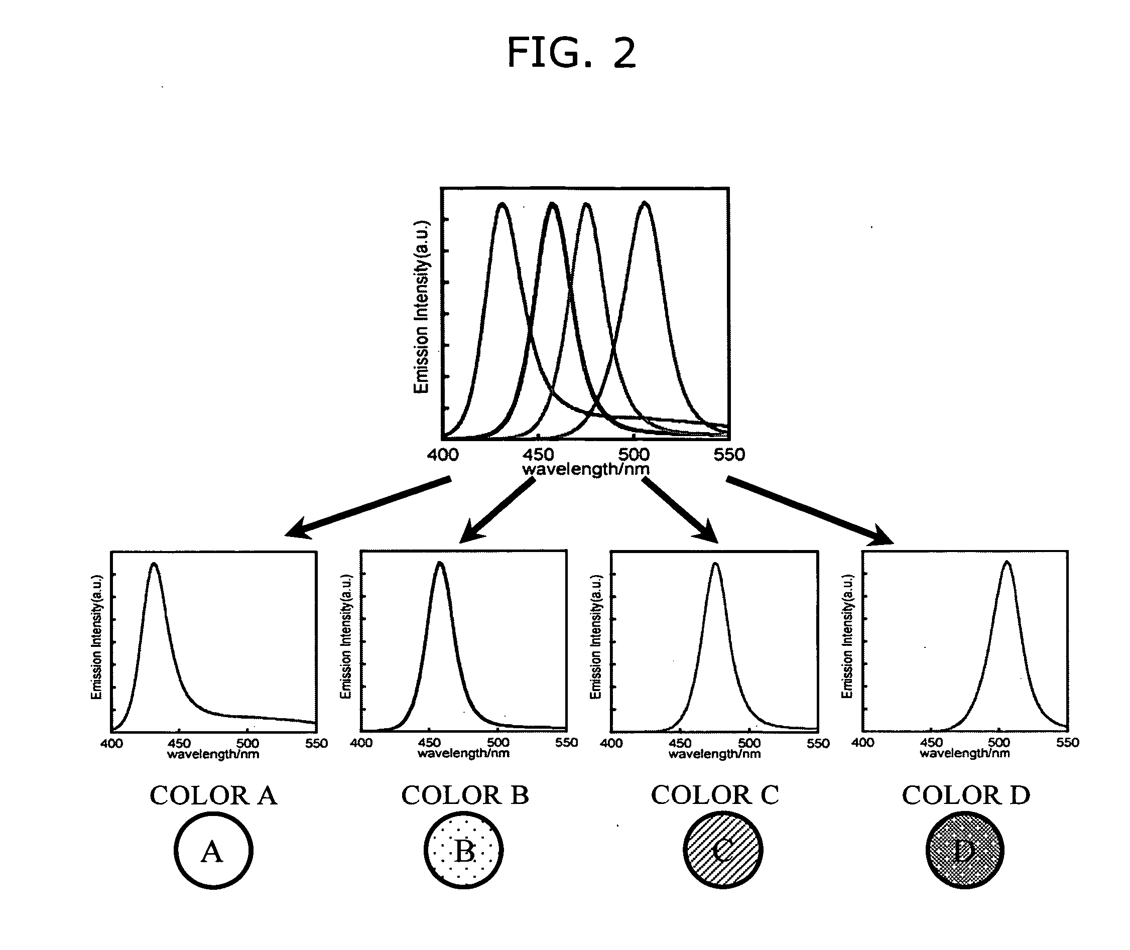
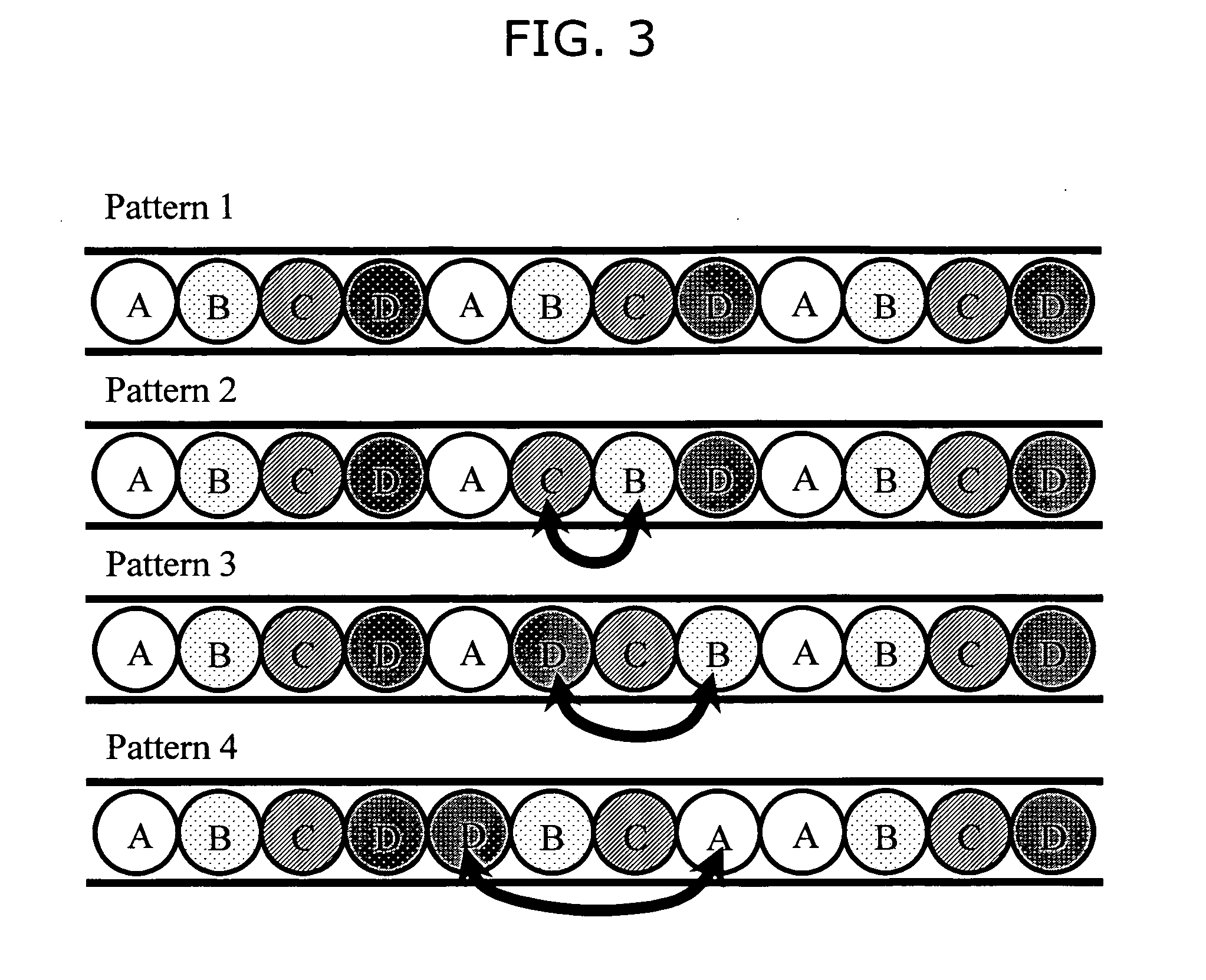
[0021] In the following, an embodiment of the present invention is described specifically with reference to the drawings. The following description uses an example in which the arrangement or the order of beads that have embedded semiconductor nanoparticles as pigments is identified regarding the probe array technology. However, the present invention is not limited to this, but widely applied for identifying various materials. Although the example pertains to the identification of the beads arranged one-dimensionally, the same identification applies even if the arrangement of the beads is two-dimensional.
[0022] In the present invention, semiconductor nanoparticles are used for description, since the semiconductor nanoparticles are preferably coloring pigments, for example, used in the process of coloring the beads.
[0023] The semiconductor nanoparticles are characterized in that they emit narrow and strong fluorescence at the full width at half maximum (FWHM). Also, various fluores...
PUM
| Property | Measurement | Unit |
|---|---|---|
| Color | aaaaa | aaaaa |
Abstract
Description
Claims
Application Information