Spatially resolved electromagnetic property measurement
a technology of electromagnetic properties and spatial resolution, applied in the direction of mechanical roughness/irregularity measurement, magnetic field measurement using permanent magnets, instruments, etc., can solve the problems of reducing accuracy, complicating data interpretation, and not yielding spatially resolved information,
- Summary
- Abstract
- Description
- Claims
- Application Information
AI Technical Summary
Problems solved by technology
Method used
Image

Examples
Embodiment Construction
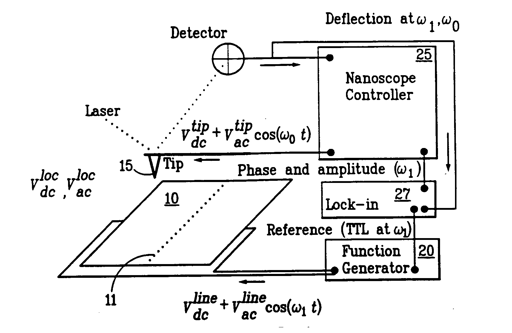
[0037]FIG. 1 illustrates a block diagram of a measurement system in accordance with an embodiment of the invention. As shown in FIG. 1, the local impedance of a sample 10 is determined across a grain boundary 11. A bias is laterally applied to the sample 10, across the grain boundary 11, and the deflection of a cantilevered tip 15 is measured. Tip 15 may be magnetic or non-magnetic. For determining grain boundary impedance, tip 15 is typically non-magnetic. The sample bias is applied with a function generator 20. The magnitude and phase of the deflection of cantilevered tip 15 are measured with a conventional atomic-force microscope (AFM) controller 25 (Nanoscope-III, Digital Instruments, Santa Barbara, Calif.). Lock in amplifier 27 is coupled to function generator 20 and AFM controller 25. AFM controller 25 may include a processor for processing measurements taken from tip 15; alternatively a separate processor may be coupled to AFM controller 15.
[0038] Tip 15 traverses the tip al...
PUM
 Abstract
Description
Claims
Application Information
 - R&D Engineer
- R&D Manager
- IP Professional
- Industry Leading Data Capabilities
- Powerful AI technology
- Patent DNA Extraction
Browse by: Latest US Patents, China's latest patents, Technical Efficacy Thesaurus, Application Domain, Technology Topic.
© 2024 PatSnap. All rights reserved.Legal|Privacy policy|Modern Slavery Act Transparency Statement|Sitemap