Differential input receiver

a receiver and input technology, applied in pulse manipulation, pulse technique, baseband system details, etc., can solve the problem of higher potential for noise-induced interference, and achieve the effect of constant symmetrical hysteresis

Inactive Publication Date: 2005-08-25
STMICROELECTRONICS PVT LTD
View PDF4 Cites 4 Cited by
  • Summary
  • Abstract
  • Description
  • Claims
  • Application Information

AI Technical Summary

Benefits of technology

[0010] The present invention also provides a method for improving a differential input receiver to provide constant symmetrical hysteresis over a wide input signal range, comprising connecting together the common input terminals of a pair of complementary differential comparators, attaching the current supply / sink terminals of a pair of series connected complementary current mirrors to the output terminals of the corresponding differential comparator, connecting a switched controlled resistance across each differential pair transistor in each differential comparator having its control terminal connected to the output terminal of its corresponding differential pair transistor, and connecting a pair of series connected inverting buffers to a common output of the differential comparators to provide the final output, the individual buffer outputs being fed back to the switch terminals of said controlled resistance in a manner that provides positive feedback, thereby providing equal rise-time, fall-delay and transition times in the output signal.

Problems solved by technology

As the signaling speed is very high, the potential for noise induced interference is higher than for the normal case.

Method used


Image

  • Differential input receiver
  • Differential input receiver
  • Differential input receiver

Examples


case 1

HIGH Transition

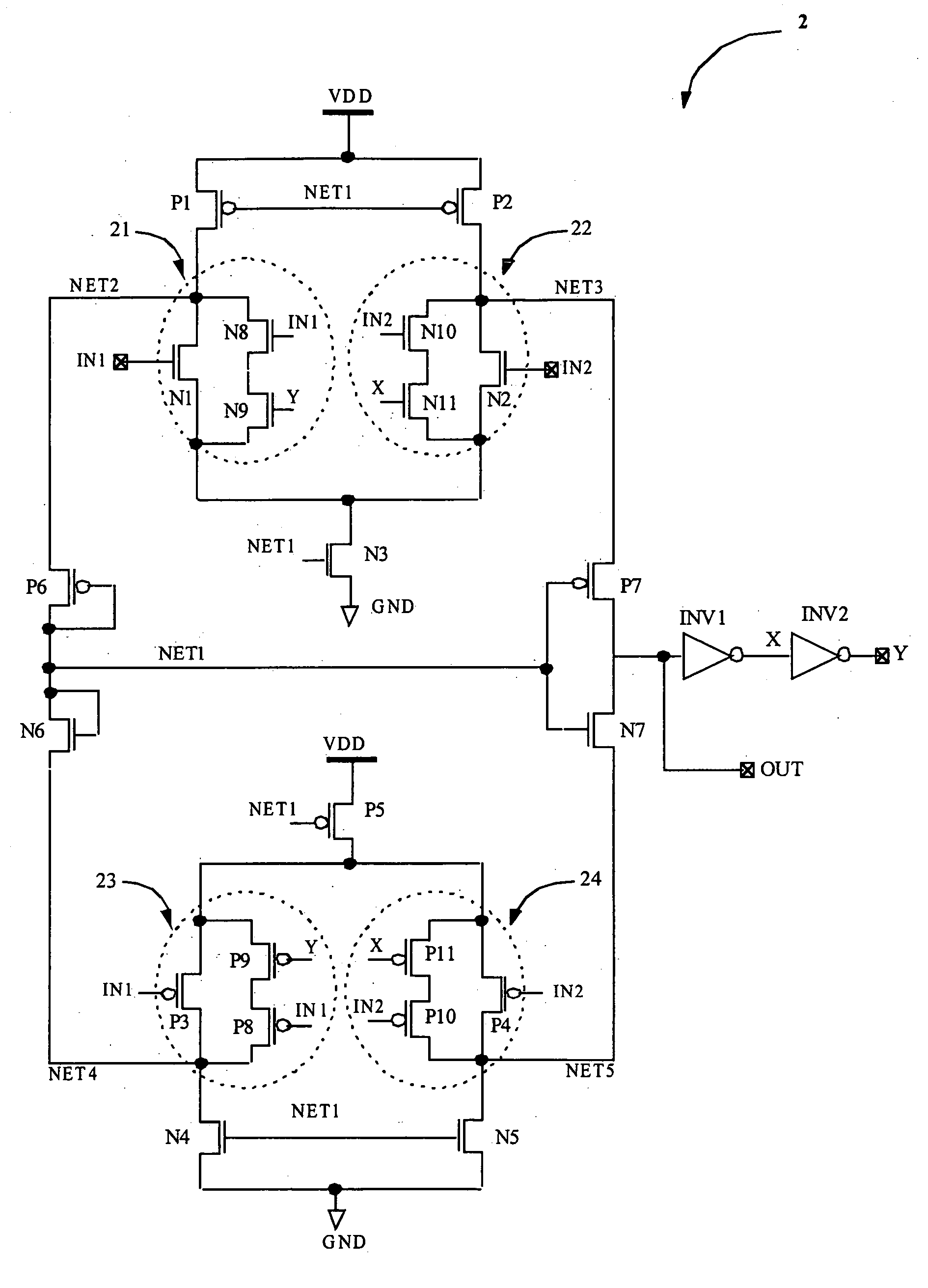
[0022] Initially IN12 and OUT=LOW so X=1 and Y=0. In this case, for NMOS differential amplifier, transistor N9 is OFF, cutting off the current path to transistor N8. Also transistor N11 is ON, hence transistor N10 is in parallel with transistor N2. As IN1 is less than IN2, the resistance of N2 is less than N1. As transistor N10 is in parallel with transistor N2, the effective resistance of branch 22 becomes much smaller than that of branch 21. As a result, the current through branch 22 is much greater than the current through branch 21. Now if IN1 increases and IN2 decreases, the resistance of N1 decreases and resistance of N2 increases. When IN1 and are equal IN2, the resistance of transistors N1 and N2 are equal but still X=1 and Y=0, this keeps transistor N10 in parallel with N2 and N8 is cut off, so the effective resistance of branch 22 is still less than branch 21. On further increase in IN1, say IN1 is just less than VTH (IN1˜VTH), the resistance of branch 21 be...

case 2

o LOW Transition

[0025] Assuming, IN1>IN2 initially and OUT=HIGH. So X=0 and Y=1. As IN1>IN2, in NMOS differential amplifier the resistance of transistor N1 is less than that of transistor N2. Moreover as Y=1 and X=0, which makes transistor N9 ON and transistor N11 OFF, so that transistor N8 comes in parallel with transistor N1 while transistor N10's path is cut off. So the effective resistance of branch 21 is much less than that of branch 22. Hence the current through branch 21 is greater than that in branch 22 which keeps OUT at HIGH, X=0 and Y=1.

[0026] If IN1 decreases and IN2 increases, the resistance of transistor N1 increases while that of transistor N2 decreases. But still X=0 and Y=1, which holds transistor N9 ON and transistor N11 OFF. This keeps transistor N8 in parallel with transistor N1 while transistor N10's path is cut off. So the effective resistance of branch 21 is still less than that of branch 22 and current through branch 21 is still greater than branch 22.

[0027...


PUM


Abstract

The differential input receiver provides constant symmetrical hysteresis over a wide input signal range. The differential input receiver includes a pair of complementary differential comparators having common input terminals, a pair of series connected complementary current mirrors each having source terminals driven by the output terminals of the corresponding differential comparator, a pair of transistors connected in series across each differential pair transistor in each differential comparator to form a potential divider across it, and a pair of series connected inverting buffers connected to a common output of the differential comparators to provide the final output. The individual buffer outputs are fed back to the control terminals of the series connected transistors in a manner that provides positive feedback thereby providing equal rise-time, fall-delay and transition times in the output signal.

Description

FIELD OF THE INVENTION [0001] The present invention relates to the field of high speed differential signaling, and, more particularly, to a differential input receiver with hysteresis. BACKGROUND OF THE INVENTION [0002] Hysteresis characteristics are used in digital logic circuits to reduce / eliminate input noise to prevent false signals and glitches. A differential input receiver is essentially used for high-speed differential signaling. As the signaling speed is very high, the potential for noise induced interference is higher than for the normal case. Further differential IO standards generally require a low voltage input swing, e.g. for Low Voltage Differential Signals (LVDS) the minimum input voltage swing is 100 mV, as a result any small noise in the input can have a significant effect. For this reason, IEEE standard 1596.3-1996, for LVDS for Scalable Coherent Interface (SCI) recommends a minimum of 25 mV hysteresis in the LVDS receiver. Since LVDS signaling can operate over a ...

Claims


Application Information

Patent Timeline
Patent Type & Authority Applications(United States)
IPC IPC(8): H03K3/3565H03K5/08H04L25/02
CPCH03K3/3565H04L25/0292H04L25/0272H03K5/084
Inventor SHARMA, MANOJ KUMARKASANYAL, SUNIL CHANDRANARWAL, RAJESH
Owner STMICROELECTRONICS PVT LTD
Why Eureka
Try Eureka